The concept of misunderstanding does not apply. If something is misunderstood it would imply you could change it and advance to a better place. This has not been the goal of this thread for weeks.
Hey man, I'm tryin'. Why not help instead of grouse?
Long before.
When? Who?
I AM one of the "villagers" that can see the CFA's differences in both
real life and simulation.
Bode responses are truly different , much faster slew. But , I never wrapped
my head around what actually is happening.
I really like CFA's , they can simplify a design and give phenomenal
results.
I appreciate the effort of this "debate" , maybe I can further my understanding
beyond "magic" (sarcasm). 🙄
PS - in the former thread ,CFA vs. VFA became almost "religious" , the villagers
became angry. wow!!
Edit - diamond diff. ?? Nakamichi amps in the 70's , there is a thread in DIYA ...
OS
Last edited:
Harris had the first IIRC good NPN/PNP process (DI).Hey man, I'm tryin'. Why not help instead of grouse?
When? Who?
Please, this thread is a pee-peeing contest, so make an argument one way or the other that leads to an improved circuit topology based on a new understanding of what so called current feedback really is or isn't.
Last edited:
Harris had the first IIRC good NPN/PNP process (DI).
Did they use it to make a diamond diff configuration? If so, do you recall when?
Please, this thread is a pee-peeing contest, so make an argument one way or the other that leads to an improved circuit topology based on a new understanding of what so called current feedback really is or isn't.
So you assert that the remaining significant contributors to this thread are engaging in public urination.
As to your suggestion, if there is no common understanding, how can anyone assess whether a proposed circuit is an improvement?
And if you don't like the way the thread has pro- or de-gressed, why not just bug out? I honestly can't figure what possible positive effects folks could expect from contributions which have devolved to the point of simply jeering at the rest of us from the sidelines.
In the absence of a response, I'm trying to guess what is bothering you about the model.
Are you objecting to the physical existence of Z?
You can measure an impedance between op amp inputs which might or might not be very large, but which (with the possible exception of CMOS gates unprotected by ESD diodes) is not infinite. A current must flow through this impedance to result in a non-zero vd. Generally speaking, an op amp output is a voltage. It is therefore axiomatic that there must exist a physical mechanism corresponding to Z.
If I am interpreting your statement correctly, then I agree about equivalence in most VFAs. But surely not to a CFA - its two inputs are quite different.
But regardless, my model makes no assumptions about the equivalence or non-equivalence of the inputs; it accommodates both possibilities.
Unless you can be more specific about your objections, I encourage you to reconsider your response to Posts 2548 and 2563.
I don't dispute the calculation, but the model.
Are you objecting to the physical existence of Z?
You can measure an impedance between op amp inputs which might or might not be very large, but which (with the possible exception of CMOS gates unprotected by ESD diodes) is not infinite. A current must flow through this impedance to result in a non-zero vd. Generally speaking, an op amp output is a voltage. It is therefore axiomatic that there must exist a physical mechanism corresponding to Z.
So, with the exception of the sign the two inputs are equivalent, I think you have to have to refine your model.
If I am interpreting your statement correctly, then I agree about equivalence in most VFAs. But surely not to a CFA - its two inputs are quite different.
But regardless, my model makes no assumptions about the equivalence or non-equivalence of the inputs; it accommodates both possibilities.
Unless you can be more specific about your objections, I encourage you to reconsider your response to Posts 2548 and 2563.
I AM one of the "villagers" that can see the CFA's differences in both ...
Edit - diamond diff. ?? Nakamichi amps in the 70's , there is a thread in DIYA
OS
Hi ostripper, I searched for that Nakamichi thread but couldn't find it. In the 70's they must have implemented it with discretes, transistors/diodes with series degenerative resistors to deal with the lack of matching.
Last edited:
Contributors to and readers of this post will doubtless be quite interested in the newest comment that appeared today at https://www.edn.com/design/analog/4458753/In-defense-of-the-current-feedback-amplifier . The comment is the first in the list.
Sergio proved it is a CFA.
But after the article , the discussions devolved into a similar discourse.
Some will never believe. Is it futile to try ?
OS
But after the article , the discussions devolved into a similar discourse.
Some will never believe. Is it futile to try ?
OS
Contributors to and readers of this post will doubtless be quite interested in the newest comment that appeared today at https://www.edn.com/design/analog/4458753/In-defense-of-the-current-feedback-amplifier . The comment is the first in the list.
Wow. That's all I can say.
If this isn't a wild story, I don't know what is. MK says that someone was impersonating him! He got in touch with EDN, and they took down the post. I can confirm it's gone.
Contributors to and readers of this post will doubtless be quite interested in the newest comment that appeared today at https://www.edn.com/design/analog/4458753/In-defense-of-the-current-feedback-amplifier . The comment is the first in the list.
Thank you for the link.
This is a very good example of circular reasoning.
1) Make a CFA model with a perfect input buffer as a general CFA model
2) Analyze a schematics with the ideal model properties
3) Generalize the conclusions.
Example :
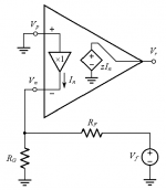
Let us investigate the physical meaning of T via return-ratio analysis [3]. As depicted in Figure 3, to apply this technique we: (a) ground the signal input to put the circuit in its dormant state, (b) break the loop at the output of the dependent source, (c) inject a test signal Vf into the feedback network, (d) find the signal Vr returned by the dependent source, and then let
Since the input buffer keeps Vn = 0, RG draws no current, so we must have In = (0 – Vf)/RF = –(1/RF)Vf, indicating that what comes back from Vf is only current and no voltage. It stands to reason to refer to this type of feedback as current feedback.
This is just wrong.
As CFA input buffer is not perfect (gain is less than 1 and output impedance is not 0), Vn is different of 0, and RG draws a current which is not 0.
vn = -vout/A where A is the amplifier voltage gain.
It is not possible to conclude that the type of feedback is current.
Attachments
Thank you for the link.
Before commenting on a new matter, would you be so kind as to reply to Post 2579? (This is an extension of what started with 2548 and continued with 2575 into 2579.)
I still think that if we want to prove that the feedback type around an amplifier is current or voltage, we have to show a schematics or a simulation with current sources for current feedback and voltage sources for voltage feedback.
It is what I tried to do, with a CFA in inverted mode as a first step.
CFA in inverted mode is not a classical configuration but it is simple to analyze.
In order not to use a model from a CFA constructor or a too simplified personal model, I design one with bipolar transistors BC550C and BC560C. It is not the best but it works.
I simulate a classical inverted config with 2 resistors and I compare with :
- a config where inverting input is connected to 2 current sources, one emulating Rf, the other one emulating Rg, driven by v(in) v(out) and v(em)
- a config where inverting input is connected to a voltage source driven by a linear combination of v(in) and v(out)
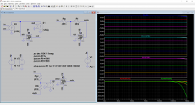
Results are summerized in attached picture.
I plot the gain of each config and the ratio of voltage or current config gains with the classical one, with Rg variation from 1 ohm to 100kohm.
There are no significative difference between the 3 configurations.
I think the differences on the ratio at frequency greater than 100kHz are caused by the different impedances viewed from the inverting input.
So, before more investigation, I am tempted to say that, in inverted mode, CFA feedback type can be analyzed as well as voltage or current feedback.
It is what I tried to do, with a CFA in inverted mode as a first step.
CFA in inverted mode is not a classical configuration but it is simple to analyze.
In order not to use a model from a CFA constructor or a too simplified personal model, I design one with bipolar transistors BC550C and BC560C. It is not the best but it works.
I simulate a classical inverted config with 2 resistors and I compare with :
- a config where inverting input is connected to 2 current sources, one emulating Rf, the other one emulating Rg, driven by v(in) v(out) and v(em)
- a config where inverting input is connected to a voltage source driven by a linear combination of v(in) and v(out)
Results are summerized in attached picture.
I plot the gain of each config and the ratio of voltage or current config gains with the classical one, with Rg variation from 1 ohm to 100kohm.
There are no significative difference between the 3 configurations.
I think the differences on the ratio at frequency greater than 100kHz are caused by the different impedances viewed from the inverting input.
So, before more investigation, I am tempted to say that, in inverted mode, CFA feedback type can be analyzed as well as voltage or current feedback.
Attachments
I still think that if we want to prove that the feedback type around an amplifier is current or voltage, we have to show a schematics or a simulation with current sources for current feedback and voltage sources for voltage feedback.
This is exactly what Post 2548 does. But it applies the sources wholly within the loop. These sources make no changes in any circuit impedance, so the two tests test the same circuit. Now we can directly determine the voltage and current gains around the loop of the one circuit of interest. These have direct implications for voltage and current feedbacks.
When you excite with external sources as you have done, you identify the closed loop gains of the amplifiers you are testing. But these are not voltage and current loop gains. Your tests give us no way to identify these parameters. In addition, your tests are testing two different circuits - voltage and current sources have very different impedances. So there's really no justification for trying to compare the loop gains even if we could measure them.
In order not to use a model from a CFA constructor or a too simplified personal model, I design one with bipolar transistors BC550C and BC560C. It is not the best but it works.
This is fine, but you need to include models for all transistors you use in your asc file which are not native to the LTSpice application. When I open your file, I can see the BC550 and BC560 transistors because I happen to have models for them. But the other four transistors you use, whatever they are, come up blank for me.
Thank you for the link.
This is a very good example of circular reasoning.
1) Make a CFA model with a perfect input buffer as a general CFA model
2) Analyze a schematics with the ideal model properties
3) Generalize the conclusions.
Example :
Let us investigate the physical meaning of T via return-ratio analysis [3]. As depicted in Figure 3, to apply this technique we: (a) ground the signal input to put the circuit in its dormant state, (b) break the loop at the output of the dependent source, (c) inject a test signal Vf into the feedback network, (d) find the signal Vr returned by the dependent source, and then let
Since the input buffer keeps Vn = 0, RG draws no current, so we must have In = (0 – Vf)/RF = –(1/RF)Vf, indicating that what comes back from Vf is only current and no voltage. It stands to reason to refer to this type of feedback as current feedback.
This is just wrong.
As CFA input buffer is not perfect (gain is less than 1 and output impedance is not 0), Vn is different of 0, and RG draws a current which is not 0.
vn = -vout/A where A is the amplifier voltage gain.
It is not possible to conclude that the type of feedback is current.
It has been pointed by MK, Syn08 in this thread, and many other authors, I think, that the fundamental mistake in the CFA analysis relies in considering the input buffer as perfect voltage source and getting conclusions from what then happens in open loop mode with signal injected in Rf
A fair analysis in closed loop mode is much more fructuous as it lifts the veil on the mystery of the low impedance of the inverting input having almost no effect on the voltage division by the feedback network.
It has been pointed by MK, Syn08 in this thread, and many other authors, I think, that the fundamental mistake in the CFA analysis relies in considering the input buffer as perfect voltage source...
That would be a fair assessment if it were the case. However, if one were to only read the entire article at https://www.edn.com/design/analog/4458753/1/In-defense-of-the-current-feedback-amplifier, one would find that it is not.
And again I must ask you, would you be so kind as to reply to Post 2579? (This is an extension of what started with 2548 and continued with 2575 into 2579.)
This is exactly what Post 2548 does. But it applies the sources wholly within the loop. These sources make no changes in any circuit impedance, so the two tests test the same circuit. Now we can directly determine the voltage and current gains around the loop of the one circuit of interest. These have direct implications for voltage and current feedbacks.
When you excite with external sources as you have done, you identify the closed loop gains of the amplifiers you are testing. But these are not voltage and current loop gains. Your tests give us no way to identify these parameters. In addition, your tests are testing two different circuits - voltage and current sources have very different impedances. So there's really no justification for trying to compare the loop gains even if we could measure them.
I know what I do is completely different of what you do.
It is different because I disagree with the calculation you do.
I disagree on your definition of what you call "current loop gain".
The current gain of a device is the ratio between output current and input current. This ratio depends of the output impedance, the load impedance and the input impedance.
What you calculate is the ratio (I(Rf)-I(Rg))/I(in-), which unless demonstration can't be considered as "current loop gain".
A current loop gain would be the ratio between an open loop current gain and a closed loop current gain, and I doubt it corresponds to your definition.
The aim of what I do is not to compare voltage loop gain and what you call or what would be "current loop gain" but simply to see if a CFA can work with pure voltage or pure current feedback.
My simulations show that a CFA perfectly works with the 2 configurations.
With the current sources configuration, absolutely no voltage is applied on inverting input so we are clearly in presence of current feedback.
With voltage source, I impose a voltage at inverting input level without any current consideration so we are in presence of pure voltage feedback.
It would be interesting to estimate the ratio of current or voltage feedback in the real configuration according to your criteria which involve voltage or current loop gain. To do that we have to agree on their definition and calculation.
Sorry, I use j505 current source. Model is attached.This is fine, but you need to include models for all transistors you use in your asc file which are not native to the LTSpice application. When I open your file, I can see the BC550 and BC560 transistors because I happen to have models for them. But the other four transistors you use, whatever they are, come up blank for me.
Attachments
A fair analysis in closed loop mode is much more fructuous as it lifts the veil on the mystery of the low impedance of the inverting input having almost no effect on the voltage division by the feedback network.
You are stating the obvious and the uncontested. I know of no one in this thread who claims that there is no voltage feedback in a CFA. But you and those who think like you claim that there is no current feedback. Your argument seems to be akin to that of a man who says, "See, I am hungry. Therefore, I cannot also be thirsty!"
Post 2548 shows that proving that claim will be problematic. It points out that non-theoretical (physical) CFAs and VFAs with feedback loops, whose input signal sources are set to zero, present a ground-referenced, finite, non-zero impedance rd at their non-inverting inputs. A second finite nz impedance zf is presented to that input by the feedback network. By inserting (separately) a voltage or current signal into the forward path at the inverting input without disturbing any impedances in the circuit, it is shown that current and voltage gains around the loop are also finite nz.
In response to those (separate) signal insertions, the loop returns other signals to the same point - that is, there is feedback, both current and voltage.
I know what I do is completely different of what you do. It is different because I disagree with the calculation you do.
I disagree on your definition of what you call "current loop gain".
I presume that you do not deny the existence of a feedback loop, and that there is gain around that loop. But this is different from the "transfer" gain which is the relationship between the input and output signals. Consider for simplicity a voltage amplifier with a zero output impedance. If the open loop gain is a and the feedback network transfer function is b, then the loop gain is L = a b. But the transfer gain G of the amplifier is different: G = a / ( 1 + a b ).
Since you reject my definition of and means of testing L, how would you define and test it?
The current gain of a device is the ratio between output current and input current. This ratio depends of the output impedance, the load impedance and the input impedance.
Yes. This is akin to G (but for current), not L.
What you calculate is the ratio (I(Rf)-I(Rg))/I(in-), which unless demonstration can't be considered as "current loop gain". A current loop gain would be the ratio between an open loop current gain and a closed loop current gain, and I doubt it corresponds to your definition.
"unless demonstration"? please explain.
You are saying that a loop gain is the ratio of two loop gains. This is a useless, circular definition.
A feedback amplifier has a loop, an input signal, an output signal, and a load. There is the transfer gain, which relates the input and output signals, and a loop gain, which is defined and tested as I have shown. These are two different things. Again, how would you define and test loop gains, voltage and current?
A voltage appears at the non-inverting input of the current source configuration due to the non-zero input impedance. We can argue about whether it is "applied", but it certainly arises....With the current sources configuration, absolutely no voltage is applied on inverting input so we are clearly in presence of current feedback.
With voltage source, ... we are in presence of pure voltage feedback.
And a current flows into the input of what you refer to as the voltage source (configuration). In that configuration, I(en) = I(in) - I(outn). Denying this relationship denies Conservation of Current, which I doubt that you are prepared to do. The relationship between I(en) and I(outn) establishes current feedback. This is clearly not "pure voltage feedback."
Alternatively, you can find the Thevenin equivalent of In, Outn, Rf and Rg. The voltage source VT = (Rf In + Rg Outn) / (Rf + Rg). VT is connected to en by Rfg = Rf Rg / (Rf + Rg). Surely you will not deny Thevenin's Theorem! A current flows between VT and en. Outn contributes to VT. This establishes a relationship between I(en) and Outn, one of current feedback. Again, this is clearly not "pure voltage feedback."
Thanks for the J505 current source. Kindly post the CR en courant.asc file.
Last edited:
- Home
- Amplifiers
- Solid State
- Current Feedback Amplifiers, not only a semantic problem?