Hi, I am planning a revision to this board utilising more of what I've learned from my recent DAC designs, namely trying to provide a more solid ground return and I may also wish to leave space for larger coupling capacitors. This may be a while coming since I am more busy now with other stuff but if I get the board manufactured there will be 3 produced, so I will likely be selling off 2 🙂
Looks awesome.. Cant wait to see the result..
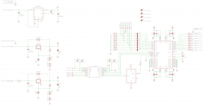
Did you listen to the pcb shown on page 3? In my oppinion and what I know about DAC Designs this layout has a very bad gnd design. Please note that THIS is the most important point on such a circuit! I did the same mistake once and had a lot of control signal noise in the audio signal.
Did you listen to the pcb shown on page 3? In my oppinion and what I know about DAC Designs this layout has a very bad gnd design. Please note that THIS is the most important point on such a circuit! I did the same mistake once and had a lot of control signal noise in the audio signal.
I was hoping for a new revision ;o)
How coincidental, I have been working on this new layout since Sunday! It uses a near continuous ground plane and takes capacitors with 22.5mm pitch (10uF film is possible).
A better digital regulator is employed here and the high ripple-rejection implementation of the 317/337 pair is used here again as in my DAC design.
I have removed the level translator actually, only because I realise now that most my peripherals will be 3.3V logic anyhow, so it makes more sense for me to use either a 3.3V uC or level translation on the uC board.
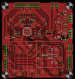
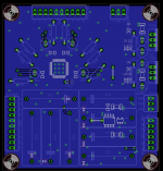
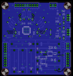
This design is a bit hard to read, you're seeing the top, but actually you'd mount it upside down. From the top view of a mounted board you'll just see headers, capacitors and the TH resistors. This works out well for space efficiency, you can see the space under the caps is used for signal routing and the 3.3V regulator, but at the same time the sensitive capacitors are shielded by the ground plane from control line noise etc.
I hope this can get close to the performance of the device, which is of course excellent 🙂
A better digital regulator is employed here and the high ripple-rejection implementation of the 317/337 pair is used here again as in my DAC design.
I have removed the level translator actually, only because I realise now that most my peripherals will be 3.3V logic anyhow, so it makes more sense for me to use either a 3.3V uC or level translation on the uC board.
This design is a bit hard to read, you're seeing the top, but actually you'd mount it upside down. From the top view of a mounted board you'll just see headers, capacitors and the TH resistors. This works out well for space efficiency, you can see the space under the caps is used for signal routing and the 3.3V regulator, but at the same time the sensitive capacitors are shielded by the ground plane from control line noise etc.
I hope this can get close to the performance of the device, which is of course excellent 🙂
Attachments

Hi Dr_EM,
A few things...
1. Are input caps really required? They are huge!
2. Why the massive resistors on the outputs? You've used SMD parts elsewhere, why not just use 1206 resistors?
3. I haven't seen that LM3x7 arrangement before. You've used two diodes in place of one of the divider resistors? And only one protection diode?
That's a strange way of doing it, why not just put the CS3318 and 3.3V regulator on the bottom layer?This design is a bit hard to read, you're seeing the top, but actually you'd mount it upside down.
I just noticed this thread today 😉
my take on this kind of board would be to have both input and output buffering (op-amps). I've posted on other threads for the 3318 why this is important.
I also suggest trying a TI TPS7A30 style regulator. here, I'm using an easy eval board but if I ever get around to makeing a real green board, I'd design for the TI chips and put them as close to the cirrus chip as I could, following the layout that TI suggests for their reg chips.
finally, I personally prefer to use spi instead of i2c and since spi is not bi-directional (lines) you can use simple opto-couplers for isolation. its not strictly needed but I think every bit helps, when you get isolation from the cpu system and the audio chips. spi is also easier to deal with since you can run it at any speed, fast or slow, and bit-bang it via software from any controller.
oh, one more idea: I'd also have a small local controller on that board that converts an 'easier' protocol on the outside (user side) to the cirrus protocol. I'd pick a simple ascii interface that has each request and reply ending in a newline, so you could simply test things with a terminal program and a usb/ttl serial adapter.
Attachments
Hi guys,
I can add,
I agree the SPI bus is the easiest to isolate probably the best to use.
If you use i2c, then I think NXP makes isolators, if you think that the digital noise will get into the analog domain.
Also ADI ADuM7440_7441_7442
If you have more than one i2c slave device then dedicate one i2c channel only to the 3318 and use another i2c channels to service those devices. Obviously need a device with more than one i2c channel or use a sw i2c means.
Can add using FTDI virtual USB UART device, FT232R, works flawlessly. I use it for remote control and for the bootloader, which is a nice to have, to make updates so easy.
+1 for the FTDI chip, works everytime, i think i have pretty much used it in everything i have built..
That's quite a bit of feedback! I'll try to address some of the points now.
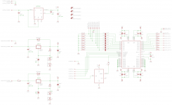
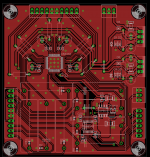
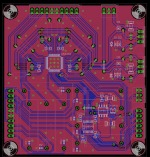
Hi, the input caps are as recommended in the datasheet, 10uF, and ideally we want film caps here, even though the voltage across them should be practically nil. This is a common size of 10uF low voltage film cap and reasonably cheap from Farnell etc. It isn't so big, bear in mind the board is still a very modest 74x72mm, (9" square for cost analysis).
Those resistors are standard 1/4W and are the main difference between this and my original design. Their use leaves enough space to route power and signal input to the Cirrus on the top layer alone. The holes they make in the ground plane shouldn't be too much of an issue and they are very common/cheap.
The LM317/337 arrangement is detailed here, Avro Arrow linked it in my DAC thread. The PCB allows you to thermally couple the diodes too, on breadboard I found diodes coupled in this way held a totally stable output voltage. I will try to get measurements of ripple rejection and noise vs the common arrangement. The filter capacitor of 22uF doesn't really warrant the second protection diode but because of the 100uF output electros I have D3 and D6.
The upside down board view isn't intentional, it just developed that way and I can't see an easy way to reverse it in Eagle? I'll just be sure to put any board name/number on the bottom layer so it's visible when mounted 🙂
With regard to the other comments, I feel as though you are hoping to operate the board almost stand-alone, with just a PSU? That wasn't the design intent for me, since this board sits between a buffered DAC output and a balanced line driver stage in my proposed setup. The system is then controlled by on-board microcontroller. I do like the idea of a simple serial interface for testing though, it just depends how much board space it takes up and how much it actually simplifies setup.
The voltage regulators, I had a good search for alternatives to LM317/337 and never found those! They can supply enough current for this board, though possibly marginal on the DAC board. I doubt there is any real world benefit of using such a precision regulator compared to the arrangement currently shown, since the CS3318 already has good PSRR, but we'll see when I hopefully get measurements of the LM317/337.
Isolators and level translation I will look into. I can't help feeling that using an opto-coupled setup actually just creates larger switching spikes in the system since you need to drive several milliamps into the LEDs when compared to virtually nothing into a high impedance input. I guess it comes down to whether you have an isolated ground/PSU on the driving end.
Thanks for your comments! 🙂
Hi Dr_EM,
A few things...
1. Are input caps really required? They are huge!
2. Why the massive resistors on the outputs? You've used SMD parts elsewhere, why not just use 1206 resistors?
3. I haven't seen that LM3x7 arrangement before. You've used two diodes in place of one of the divider resistors? And only one protection diode?
That's a strange way of doing it, why not just put the CS3318 and 3.3V regulator on the bottom layer?
Hi, the input caps are as recommended in the datasheet, 10uF, and ideally we want film caps here, even though the voltage across them should be practically nil. This is a common size of 10uF low voltage film cap and reasonably cheap from Farnell etc. It isn't so big, bear in mind the board is still a very modest 74x72mm, (9" square for cost analysis).
Those resistors are standard 1/4W and are the main difference between this and my original design. Their use leaves enough space to route power and signal input to the Cirrus on the top layer alone. The holes they make in the ground plane shouldn't be too much of an issue and they are very common/cheap.
The LM317/337 arrangement is detailed here, Avro Arrow linked it in my DAC thread. The PCB allows you to thermally couple the diodes too, on breadboard I found diodes coupled in this way held a totally stable output voltage. I will try to get measurements of ripple rejection and noise vs the common arrangement. The filter capacitor of 22uF doesn't really warrant the second protection diode but because of the 100uF output electros I have D3 and D6.
The upside down board view isn't intentional, it just developed that way and I can't see an easy way to reverse it in Eagle? I'll just be sure to put any board name/number on the bottom layer so it's visible when mounted 🙂
With regard to the other comments, I feel as though you are hoping to operate the board almost stand-alone, with just a PSU? That wasn't the design intent for me, since this board sits between a buffered DAC output and a balanced line driver stage in my proposed setup. The system is then controlled by on-board microcontroller. I do like the idea of a simple serial interface for testing though, it just depends how much board space it takes up and how much it actually simplifies setup.
The voltage regulators, I had a good search for alternatives to LM317/337 and never found those! They can supply enough current for this board, though possibly marginal on the DAC board. I doubt there is any real world benefit of using such a precision regulator compared to the arrangement currently shown, since the CS3318 already has good PSRR, but we'll see when I hopefully get measurements of the LM317/337.
Isolators and level translation I will look into. I can't help feeling that using an opto-coupled setup actually just creates larger switching spikes in the system since you need to drive several milliamps into the LEDs when compared to virtually nothing into a high impedance input. I guess it comes down to whether you have an isolated ground/PSU on the driving end.
Thanks for your comments! 🙂
the optos are powered by the digital supply, not the analog supply.
I just like the idea is complete isolation between the digital controller side and the analog-based vol control chip.
it might help and I doubt it will cause any problems. on my own design, I do plan to do the opto thing.
I just like the idea is complete isolation between the digital controller side and the analog-based vol control chip.
it might help and I doubt it will cause any problems. on my own design, I do plan to do the opto thing.
I have made a portable radio/media player that has no i2c isolation. It is very quiet through sensitive speakers and phones. It has lots of clocks, so much, that they interfere with the AM radio section and I need to really isolate it with shields. Hardly hear any clock noise on a off station in FM. FM is pretty sensitive, I can receive/tune FM stations 75-100 miles away in the 20uV range with good fidelity in mono or 0% blend. I do have a deep fringe log periodic ant, a RF booster on the mast with a rotor to pin point the source.
The pcb is 4-layers due to density and to make a very quite ground. I am using a 2 step reg DC in to 5V(LM317) , 3V3(LM1086)
There is more interference from the individual ic clocks radiating than from the i2c bus.
I am using a
Si4735 radio
MAX9729 selector,volume,headphone amp
TPA3100D2 25W class D
PCM2902B USB codec
BU9458 USB MP3 player
PCA8565 rtc
FT232RL
xm192a3
4x40 LCD
I guess if you want to wring the last few drop of performance out of your design, isolate the com link and separate ground planes. Multi-layer ground planes, do make a big/huge difference and in my case do not require isolation of i2c or grounds.
I area fill all layers in a ground plane. You can get real fancy and have very thin dielectric spacing, between power/ground planes, to act as decoup caps. Works well in high speed digital designs.
As an experiment it would be good to try both methods and measure/test the differnces.
Oh ya, you'll cringe to know I am using 1uF/50V/1210/X7R audio coupling caps 🙂 PP film would take up way to much real estate.
Cheers
With regard to the use of opto-coupling, yes the supply is digital but what you'll be doing is bringing the digital lines out from the microcontroller end over to this board (hopefully only a few cm of cable) and loading them down such that they carry several milliamps instead of a very small signal current. This makes for a relatively large loop area of higher current digital signals and implies an increased radiated noise penalty. So, it is more likely to be equal or worse depending on your cable routing and internal system layout IMO.
I may return to that old 5V tolerant logic shifter/buffer IC, not only does it give the option to run from 5V logic but since it is an older design then it should have relatively slow rise times on the logic and the reduced coupling that comes with that. We don't need this control port to run at massive frequencies and using this may help ensure the design is noise free regardless of driving logic.
I like the idea of multiple layers, it is common for professional digital and mixed signal audio boards to have upwards of 10 layers. Unfortunately, it warrants a huge cost hike for DIY quantities. A 4 layer design here would allow me to use nice analogue power planes, but for twice the cost it doesn't seem worth it. I've tried to allow guard traces around all the analogue tracks to keep crosstalk minimal and have stitched these top layer grounds at regular intervals. The PCB capacitor is an interesting concept, certainly it's used in RF design, may not be too important here though! Yes, X7R are known to add distortion, but if suitably sized as a coupling cap it may be very minimal since voltage across the cap is minimal.
Thanks all!
Hi,
Newer mcu's like the xmega have limited slew rate control for the pins. Also the lower the voltage swing, the lower the radiated/conducted noise. Basically 5V logic is obsolete, suggest to stick with either 3.3 or 2.5V logic, saves power, minimizes switching noise. Most new peripheral devices standardize on 3.3 or 2.5V logic.
I do understand even a 4 layer pcb is kinda outside the realm of DIY, but I was just providing some input as far as options and what I have done in the past.
BTW the embedded decoupling plane design was 16 layers done in 0.062" finished, but then again we were using a 1152 pin BGA Xilinx device and a whole bunch more of IDT BGA dual-port memories and a 32-bit IBM powerpc MCU. It was a 10 and 2 Gbit/s Fibre Channel/Ethernet pci test card.
Core material was ZBC-106 at 0.002"
Good Luck with your design and keep us informed as to your progress.
Rick
That's interesting about the new microcontrollers, though it's perhaps even better to have a design suitable for use with any drive logic. You're right about 5V logic being practically redundant, though I may have to do some searching to find a 3.3V OLED display, or just use level translation on that peripheral.
That sounds like a pretty serious board! When you have BGA devices and high speed logic then numerous layers become practically mandatory. That's very high speed data so you must have to pay close attention to track lengths , use of vias, track bends and characteristic impedance; a bit beyond my experience right now 😀😱
Anyhow, here's a design offering isolation from the control bus, utilising one of these clever devices:
Analog Devices ADuM7440 Product Page
There are now some low power versions too which may be superior in keeping noise levels down, though cost slightly more.
linuxworks, I think I see now where the isolation could be useful, it is where you are powering your MCU board and LCD/OLED from a totally independent supply. I wasn't planning to do this but can see how it is attractive. This design with the ADuM shouldn't burden the control lines with extra current demands. Drive from 3.3V and 5V logic is possible too, perhaps nice for testing 🙂
This board is no larger and the ground plane is still mostly solid. I'm not convinced on it being necessary, I guess now it depends how well your MCU board will handle its ground currents, but with this isolated board you can 'get away' with breadboard or stripboard MCU controllers.
Attachments
Last edited:
I have started af volume control thread where CS3318 is a part of the idea, you are very welcome to contribute to that if you feel like it:
http://www.diyaudio.com/forums/digital-line-level/248646-diy-volume-control-open-source-project.html
http://www.diyaudio.com/forums/digital-line-level/248646-diy-volume-control-open-source-project.html
On the 16-layer test card, we spent a fair bit of time doing signal integrity sim's, using IBIS models. SW tools called Interconnectix and HyperLynx(Mentor Graphics) . There is a really good Intel design guide for the 10 G serdes,
Designing SERDES Applications--82545/82546, 82571/82572 & 631xESB/632xESB Application Note--AN498
and others
That and $100K Agilent scope 🙂
Your 3318 design looks good, I'd review the gerber/drill data, if you wish to post it.
Cheers
Rick
Designing SERDES Applications--82545/82546, 82571/82572 & 631xESB/632xESB Application Note--AN498
and others
That and $100K Agilent scope 🙂
Your 3318 design looks good, I'd review the gerber/drill data, if you wish to post it.
Cheers
Rick
That's an interesting thread, lots of ideas there. Will see if there's anywhere I can help at all. Something I want in this project which I totally don't know how to do yet is a back-channel to the PC, such that remote control signals can be used to skip tracks or pause playback from the PC.
I think simulation is a big step forward in helping guarantee the proper operation of high frequency boards. And yes, a good scope will be essential when you come to testing such boards!
I've attached the gerbers and you can open them in GC Prevue with the included save if you wish 🙂
I think simulation is a big step forward in helping guarantee the proper operation of high frequency boards. And yes, a good scope will be essential when you come to testing such boards!
I've attached the gerbers and you can open them in GC Prevue with the included save if you wish 🙂
Attachments
I did some serial work that would link the preamp with a pc.
the idea, as I did it, was to have a daemon process on linux connected to 2 endpoints: a tcp socket and a serial port (usb/serial). the serial side connects to the arduino (in my case) and it does GET and SET requests over the serial line in a simple protocol.
the tcp server side can take connects from the network (or even a local webserver) and that gets you the networked remote control side of things.
I also hacked the linux vol control system (mixer) so that when you change the vol on any linux app, a hook is triggered and a serial i/o request is sent to the arduino to update the vol in the real preamp. no actual atten is done on the linux side, analog or digital; its just a control intercept.
similarly, when the user changes the knob on the preamp, an update is sent over serial to the linux daemon and he updates the mixer slider so that the user sees the 'knob' turn on the software linux side.
you could also send some ir codes over serial (relayed by the preamp) and that daemon process can know that its a FF or REW or PAUSE request and control some linux transport (like mpd).
Hi,
I use GerbTool. The design loaded fine and I do not see any show stoppers in the data.
Good Luck
Rick
I use GerbTool. The design loaded fine and I do not see any show stoppers in the data.
Good Luck
Rick
Hi,
I have a ? more on the system level. Do you know the source impedance's for each input?
If not then, as stated in the DS.
1) using (optional) a input buffer/LPF?, optional gain?
2) A L+R summer/LPF/LF shelving ckt for a sub channel?
As a suggestion, since it is big deal to get a pcb done, try to get the biggest bang for the buck, a complete stereo on a pcb.
Like say, a remote controlled pre-amp, all on a one pcb. Even the transformer/PS. The MCU section is very small additional area.
I get into the trap, that I forget/put-off packaging til I have the design up and running. Is there a final long term product, what will it look like, how will or will I use it often.
The UI is another thing, get that figured out as well. Menus? Even as far as, do I want a balance control?
Oop's how about tone controls? 🙂 Nothing, bass boost is sub channel boost?
I hope my insight helps you more than it hinders you into getting your project done.
I'll share with you a 7.1 channel pre-amp design that is halted as it got out of hand. I was not confident in my coding ability, at that time because of no experience. I made a small portable unit instead as a test bed for my coding. I am glad that I did the portable, because now I have defined the UI and have the code up and running.
BTW, I was going to use PGA2320/4311 as the V controls, you'll find them if you really zoom in on the details.
Good Luck
Rick
I have a ? more on the system level. Do you know the source impedance's for each input?
If not then, as stated in the DS.
What I am saying, have you decided against, some of these items,The addition of an input coupling capacitor will form a high-pass filter with the CS3318’s input impedance.
Given nominal values of input impedance and coupling capacitor, a 10 μF coupling capacitor will result in
less than 0.03 dB of attenuation at 20 Hz. If additional low-frequency attenuation can be tolerated, a smaller
coupling capacitor may be used.
The CS3318 requires a low source impedance to achieve maximum performance, and a source-impedance
of 600 Ω or less is recommended.
1) using (optional) a input buffer/LPF?, optional gain?
2) A L+R summer/LPF/LF shelving ckt for a sub channel?
As a suggestion, since it is big deal to get a pcb done, try to get the biggest bang for the buck, a complete stereo on a pcb.
Like say, a remote controlled pre-amp, all on a one pcb. Even the transformer/PS. The MCU section is very small additional area.
I get into the trap, that I forget/put-off packaging til I have the design up and running. Is there a final long term product, what will it look like, how will or will I use it often.
The UI is another thing, get that figured out as well. Menus? Even as far as, do I want a balance control?
Oop's how about tone controls? 🙂 Nothing, bass boost is sub channel boost?
I hope my insight helps you more than it hinders you into getting your project done.
I'll share with you a 7.1 channel pre-amp design that is halted as it got out of hand. I was not confident in my coding ability, at that time because of no experience. I made a small portable unit instead as a test bed for my coding. I am glad that I did the portable, because now I have defined the UI and have the code up and running.
BTW, I was going to use PGA2320/4311 as the V controls, you'll find them if you really zoom in on the details.
Good Luck
Rick
Attachments
Last edited:
- Status
- Not open for further replies.
- Home
- Source & Line
- Analog Line Level
- CS3318 PCB Layout