Well, just figured it is a good idea ti get the best possible starting point and make shure that the transistors I solder back in are matched well enough to close out transistor mismatch in the differential amp as a source to my problems.
Allso, I read in an amplifier handbook how the matching of differential pairs influenced distortion figures, and it was evidently a lot to gain as a Ic difference of as little as 2% could have significant impact on 2nd harmonic distortion.
Regarding the thermal drift and stability issue, both transistor pairs are placed closely together and I've used thermal compound and a piece of aluminium tubing to clamp them together so they make contact between the flat faces. this was allso recommended in the build description to prevent any imbalance due to thermal difference.
Last edited:
In this case you should use another transistors. BC550, BC560 are better because they are low noise, or 2sa970, 2sc2244.
Leon,
Interresting suggestion, but can these transistors you suggest be used as a direct replacement without any other circuit modifications??
Interresting suggestion, but can these transistors you suggest be used as a direct replacement without any other circuit modifications??
I think you can use BC550, BC560 as direct replacement, but 2sa970, 2sc2244 have another pinout.
Oh no...
I soldered back the T1-4 transistors I have just matched, and switched the amp on.
No improvement, output offset is now 180 mV.
So, at least I think I have elliminated poor differential pair matching as the root cause.
So now the question is what to check next and how to do it??😕
I soldered back the T1-4 transistors I have just matched, and switched the amp on.
No improvement, output offset is now 180 mV.
So, at least I think I have elliminated poor differential pair matching as the root cause.
So now the question is what to check next and how to do it??😕
Yupp,
Measured the current through the + and - supply, and got about 210 mA for both.
In the build description, idle current is specified at 200 mA under measurements, so I guess this is OK?
Measured the current through the + and - supply, and got about 210 mA for both.
In the build description, idle current is specified at 200 mA under measurements, so I guess this is OK?
Last edited:
Elbert, looks like you are unfortunately going around in circles on this difficult problem.
Here are some ideas I hope will help you. Firstly, lets think about 'dividing and conquering' the problem. Its unlikely that the diffierences in Vbe or Hfe on the input stage are the cause of your problem. The fully balanced topology is actually very forgiving with respect to front end device matching.
You need to isolate the problem.
1. Check that the front end current sources are working correctly - measure the collector voltage of T5 and T6 (I cannot read the circuit clearly, but these are the current source transistors in the top left hand side and the bottom left hand side). The voltage drop across the collector load resistors should be thesame to within a few hundred millivolts.
2. If these voltages are correct, next step is to check the voltage drop across the collector load resistors connected to T7 and T9. They should be similar and around 1.1V assuming the current source value of c. 2.2mA from what I can see.
Next step if this is ok is to look at whether there is a problem in the output stage. Best way to do this is to remove the output devices, and connect R23 to the top of R29. If you them measure the voltage at this point wrt to ground, you should read close to 0V +-a few hundred mV if the front end is ok and your problem is in the output stage. If you are still reading > 1V, your problem is somewhere on the front end.
I note this amplifer has an input via R5 (?). Is this the DC offset circuit? If so, what happens when you disconnect it it?
Bonsai, It does in deed seem I'm going arround in circles here, or any other direction failing to take me closer to a solution.
I shall perform the checks you have suggested and hopefully that can break this circle!
The connection at R5 is the connection point for the DC servo signal from the Servo/ protection card.
the servo is now disconnected and the amplifier card has been set up to work without a servo as per the instructions of Wahab earlier on in this thread.
Last edited:
Hi,
one of the practical advantages of this topology is an accurate DC offset balancing mechanism. A reasonably stable DC offset in the picovolt region is achievable by input device matching without DC servo or blocking cap in the feedback loop.
I would make R2 equal to R23 and insert phase compensation capacitors from the VAS outputs to the inverting input as I don`t trust the existing arrangement.
Measured the current through the + and - supply, and got about 210 mA for both
This is good and means that there are no oscillations.Now you should check the resistors.Maybe you made a mistake and soldered a wrong resistor somewhere.
Leon, it is good to know that the oscilation issue is closed, one thing less to worry about!
With respect to the resistors, I have double and tripple checked, and during assembly I allso took great care in measuring every resistor to selcet as close as possible to nominal values and match for symetry.
WuYit, untill I have positively idnetified and understood the source of trouble in this amplifier, I'm a bit hesitant to do any modifications. My base assumption is that the circuit design is sound and should be working and that there is something wrong with my particular build.
As I have not been able to find any assembly-errors, my suspicion is leaning towards a component quality (semiconductor) issue somewhere..
Bonsai,
I measured the voltage drop over the T5 and T6 emitter resistors R17 and R20, and that came to 1,104 V and 1,094 V
The voltage drop across the collector resistors R18 and R21 came to 33,1 and 33,3. Unfortunately I didn't get better resolution on these last measurements as I had to use a voltage range on the multimeter which has only 1 decimal place resolution.
Again, the resistors are very carefully selected and matched, so I don't think that could be an issue.
What could cause this difference and is it significant??
I re-did these measurements which I have done before:
R25 measured 33,6Ohms and 0,443V across, R27 measured 33,6 Ohms and 0,338V across.
Rail voltage was 46,3 volts +/-
There were no significant changes.
Last edited:
Elbert,
so from your measurements we can conclude:-
1. The current sources are ok
2. You have checked the input transistors and matched them, and we can conclude they are ok - readings are close enough
3. You have measured the volt drop across the emitter degeneration resistors in the VAS and they are not balanced.
Next steps
Can you measure the volt drop across the collector load resistors in the LTP - the ones that feed into the VAS. This is just to make sure we can put the front end LTP's out of the question as the source of the problem
Can you measure what the voltages are at the bases of the cascode transistors after that - lets just make sure there's not a problem there.
One other thing that would give this problem would be if the feedback resistor was a very high value. I assume you have put a signal on the input and the gain is correct. Can you confirm that is in fact the case?
If all of the above is ok, you then need to do what I suggested earlier and remove the output devices and close the loop from the VAS back to the inverting input. This will allow you to confirm if the problem is in the front end + VAS, or whether it is an output stage problem.
Bonsai,
thank you for your interpretations and step-by step guidance so far!
I have just measured the LTP collector load resistors:
R6= 0,137V
R7= 0,052V
R11= 0,051V
R12= 0,140V
To me this looks a bit strange..?
For the other measurements, I am not entirely sure which the cascode transistors are...😱
but I meaured tha base voltage on T7 and T9, and got 1,159V and 1,064V respectively.
Was this right??😕
I Have so far not put any signal on the input, it is only connected to ground.
With the feedback resistor, do you mean R23 of 12K??
Last edited:
I have just measured the LTP collector load resistors:
R6= 0,137V
R7= 0,052V
R11= 0,051V
R12= 0,140V
Yes, something does not look right here. I cannot read the schematic, but I think the resistors are R8,R9 (connected to T1 and T2 collectors) and R15 and R14 (connected to T3 and T4 collectors). The voltage across R8 and R15 should be the same as the the voltage on the base of T7 (for R8) and T9 (for R15).
The cascode base voltage is the voltage at the base of the MJE350 with respect to the + rail, and the other one is the base voltage of the MJE340 with resepct to the - rail.
Bonsai,
Sorry for the poor quality of the schematic, my scanner is not working with the new computer I bought, so I had to use a schematic I just happened to find on the web.
I allso realised that I didn't measure the values you actually asked for, what am I doing?? Must have been tired..
Anyway, to clarify the measurements: Emitter resistors (47 Ohm) and their voltage drops are:
T1, R6= 0,137 V
T2, R7= 0,052 V
T3, R11= 0,051 V
T4 R12= 0,140 V
Collector resistors of 1K:
T1, R8=1,165 V
T2, R9=1,120 V
T3, R13=1,070 V
T4, R14= 2,97 V
This one is interresting.. why is the voltage across The T4 collector resistor R14 2,97V??
I checked the base voltage of T8 and T10, and it measured exactly 3,64 V for both, which I guess is OK?
Last edited:
measure the voltage across the two VAS emitter resistors.
Check the Vbe of the input and VAS transistors.
Have you powered up through a bulb tester? What is the voltage on the supply rails?
Check the Vbe of the input and VAS transistors.
Have you powered up through a bulb tester? What is the voltage on the supply rails?
Hi Andrew!
So,the VAS transistors would be T9 and T7 then I guess, with Emitter resistors beeing R27 and R25..
R25: 0,440 V
R27: 0.383 V
Vbe T7= 0,717 V
Vbe T9= 0,679 V
Hmm..
Voltage on the supply rails are 45,6 V +/-. I haven't useda bulb tester, but the current draw was only 210 mA per rail, so that should be normal.
Hi Elbert
in my own amplifier measures :
R6=87 mv
R7= 88mv
R11=87mv
R12=88mv
Mr AndrewT was right when he said FIX YOUR AMPLFIERS.
I put bc 550c and 560c On Semi T1T2T3T4
and the result :500mv output offset without op177 , when i put the OP177 on board then 0V Output . ιn pin 6 OP177 I measure 1,7 volt .
I have a small problem with square wave 10khz 20khz 40khz
I think that causes the zobel net?
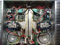
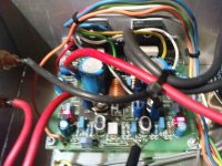
Can you show us some photos from the amplifier?
in my own amplifier measures :
R6=87 mv
R7= 88mv
R11=87mv
R12=88mv
Mr AndrewT was right when he said FIX YOUR AMPLFIERS.
I put bc 550c and 560c On Semi T1T2T3T4
and the result :500mv output offset without op177 , when i put the OP177 on board then 0V Output . ιn pin 6 OP177 I measure 1,7 volt .
I have a small problem with square wave 10khz 20khz 40khz
I think that causes the zobel net?
Can you show us some photos from the amplifier?
Attachments

Last edited:
- Status
- Not open for further replies.
- Home
- Amplifiers
- Solid State
- Crescendo Millennium offset problem