Andrew,
This is very interresting...
Just got back from the store with a set of pincer-probes and did the measurements on a working card...
Vgs on the Vgs multiplier transistor was 3,63V. Pretty close to the 3,6V I measured on the problem card (not to precise as the voltage was moving due to no-heatsink and lack of thermal coupling and stabilisation.)
Vgs on output transistor T12 was 2,02V and for T3 2,14V
Voltage between gates of T12 and T3 was 4,26V, for the problem- card, this was about 4,1V.
The pot setting for the Vgs multiplier on the good card was about 12 O' clock for a Vrs of about 45 mV.
From this, it seems to me that the Vgs multipliers on both cars behave very simmilar, but that the output transistors I have now assembled to the problem card passes a higher idle current for a given bias voltage.
I remember your comment about Vgs tollerance being very wide, and looking at the data sheet for 2SK1530 (T12), the gate-source cut-off voltage is specified at 0,8-2,8V. http://www.datasheetcatalog.org/datasheet/toshiba/2769.pdf
I can't help but think that If I have transistors from different batches that can potentially vary across such a range, thsi could explain things..
What do you think?
Assuming the above theory is more or less correct, then my problem is really the Vgs multiplier lacking the correct range to cope with the full range of manufacturing tollerances of the output transistors, not a faulty circuit.
That takes us over to your suggestion about modifying the Vgs multiplier..
I do get a bit apprehensive about replacing the specified FET transistor with a BJT. As I understand it, the thermal characteristics of T11 is important here as this is what provides stabilisation of the idle current VS temperature. You will not be surprised to hear that I feel less than qualified to select a BJT that will ensure that the thermal compensation is maintained as intended.
Would it not be possible simply to increase the value of R28 (270Ohms), thus shifting the range of the 1k pot??
PS
I allready blew up the working amp, this will be avoiding to blow up the now not-quite-working-any-longer amp.. 😉
Last edited:
you can increase 270r and 1kVR as much as you like.
The multiplier can never give out less than Vgs of the device.
The wrong device has been chosen for these lowish Vgs devices.
Normal Vertical FETs have a much higher Vgs.
It looks like the "designer" forgot to check what he was designing.
Choose any bjt. To92 can be glued to the heatsink, inserted into a drilled hole. To126 can be bolted to the heatsink, or to the top of an output device.
The bjt Ic must be able to pass the VAS current, it must have a decent hFE, it must have decent fT. None of these are critical.
Any Ic = 100mA, 40Vce0, 100MHz, hFE = 200 will do. Or a spec that exceeds some or all of these.
Have a read of Cordell, he uses mosFET output with bjt multiplier and he shows various circuit topologies that alter the temp comp factor to suit the devices that need compensating.
Andrew,
I'm wondering if we overlooked something here or if I misscommunicated any measurements??
Since my last post, I got a bit eager and decided to replace R28 with a 470 Ohm resistor..
I hooked the card up to my lab supply (with current limiter) (which can only give out 30V max), and the idle current was lower than with the 270 Ohm reisitor. With the 270 Ohm resistor, it would typically start at 60-70 Mv over the output resistor, (and rise to lack of heatsink), but now it started in the low 40's and the rise was slower.
I allso tried turning the pot a bit, and the current went up and down accordingly, i.e. no point at which turning the pot further to CCW would not yield any further reduction in idle current.
I am not sure the reduction in idle current obtained so far will be enough when I hook up to the full voltage of the amplifier supply. If not I can allways increase R28 further and see what happens.
Nevertheless, it seems, as you say, that the designer didn't check propperly in that he failed to take in to account certain tollerance extremes (assuming my output transistirs are at a tollerance extreme)
This was not quite as expected considering your last post, but nevertheless, something happened, and it seems to be bringing me in the right direction with regards to obtaining the desired idle current setting..
Hi,
are your devices anywhere near tolerance extremes?
What are the individual Vgs at what Id?
I don't think we have overlooked anything. The Vbe multiplier Vgs is simply too high to allow a wide range of output bias with low Vgs output devices.
The 1530/201 are low Vgs devices, they are designed that way when they were targeted at Audio duty.
Have a look at Vgs spec. 0.8Vgs to 2.8Vgs @ Id = 100mA & Ta=25degC.
Now look at Id vs Vgs @ Tc=25degC and 125degC for a typical 1.8Vgs @ 100mA. The Id increases ~ six fold for that 100C rise in case temperature.
If one wants to bias both N & P devices to 100mA with Rs=0r22 then the Vbias could vary between 1.64V and 5.64V
The Vbe multiplier must be able to give that range of Vbias adjustment as a minimum for setting Ib=100mA.
if one wants to turn down Ib during initial testing etc, then minimum Vbias must be well below 1.64V
Last edited:
Good question Andrew...
This is with the full power supply..
Again, T12 had a Vgs of 2,02V T13 2,14V, Id for both (based on current through output resistor) about 350mA
As you can understand this is as measured on the card.
This does not match the Vgs-Id plot of the data-sheet for 2SK1530.
According to this plot, a Vgs of 2V, should give a Id of about 2A! Am I looking at the right plot here?? 😕
Sure we haven't overlooked anything?
According to what you said, increasing the value of R28 could yield no further reduction in idle current, yet it did, and no matter how hard I sometimes wish for it, I am not cabable of magic or locally setting aside the laws of physics! 🙂
Last edited:
Well, Dinnertime now..
Later on, I'll increase the value of R28 a bit more, assmeble the card in the chassis and see if I can get the desired idel current. If so, the next step will be do do a sine-test, first with out load and then with a 16Ohm load to see if it actually works.
Later on, I'll increase the value of R28 a bit more, assmeble the card in the chassis and see if I can get the desired idel current. If so, the next step will be do do a sine-test, first with out load and then with a 16Ohm load to see if it actually works.
Hi,
your Vbias is 4.1V when the 1kVR is set to 1k.
The lowest you can get the Vbias to is 3.6Vgs (you measured that).
To get 3.6Vbias the sum of VR + 270r would need to be infinity.
You are fiddling at the edges with values that can never be practical. You changed the total Rlower from 1270r to 1470r. How much did that lower Vbias?
Vbias = [(Rupper/Rlower) +1] * Vgs
To get full adjustment ability from your amplifier, the high Vgs mosFET must be replaced with a low Vgs device. The easiest is a few cents To92 BJT.
Last edited:
yes you are using the correct plot, yes your devices are within specification.T12 had a Vgs of 2,02V T13 2,14V, Id for both (based on current through output resistor) about 350mA
As you can understand this is as measured on the card.
This does not match the Vgs-Id plot of the data-sheet for 2SK1530.
According to this plot, a Vgs of 2V, should give a Id of about 2A! Am I looking at the right plot here??
You have to learn to read the datasheet.
Vgs @ 100mA can be in the range 0.8Vgs to 2.8Vgs.
Let's assume a typical value is 1.8Vgs @ 100mA.
The manufacturer will know the average and the variation from average of every batch. from that he will have a typical batch value for Vgs.
Now using our assumed typical 1.8Vgs value look at the Id vs Vgs graphs.
The Tc=25degC is the one you should look at. What is Id when Vgs = 1.8V?
Difficult to read way down there in the curve but somewhere between 100mA and 500mA.
Lets guess it's ~ 150mA.
Now change the Tc to 125degC. What is the hot Id for 1.8Vgs, Id guess <1000mA. there's that six fold I mentioned earlier.
Now those Id are for our 1.8Vgs. find what Vgs gives exactly 100mA. That is the manufacturer's typical.
Your devices are not exactly typical. They have a tolerance that is within spec.
The curves slide slightly left for Vgs < typical and slide slightly right got Vgs > typical. It appears your devices.
If you find that the manufacturers typical is ~1.6Vgs and you have 2.1Vgs devices then the curves must be slide sideways to the right by about 0.5V
This will bring the 100mA value to coincide with the 2.1Vgs value on the Tc=25degC curve. A piece of tracing paper overlaid could be used if you really wanted to do this. We don't need to.
We can design better for device spread than the designer remembered to do by allowing for a reasonable range of device parameters.
Change the 2sk537 !
Andrew,
Regarding the T11, SK537, or its equivalent 2SK2733, I found the datasheet here:
2SK2733 pdf, 2SK2733 description, 2SK2733 datasheets, 2SK2733 view ::: ALLDATASHEET :::
It quotes a range for gate threshold between 2V to 4V.
Does this still mean that this transistor is a "High Vgs"?
Regarding the Id-Vgs curve of 2SK1530, it is clear from what you point out that I didn't read it properly!
As you understand, I'm not quite used to examining semicunductor parameters in this kind of detail, nor am I too well versed in the nature of MOSFET's..
So, it seems we are within tolerances for the transistors allbeit they are not the same for the different cards.
I just put in a 680 Ohm resistor, and this dropped the idle current even further.. I just hooked the card up to the full power supply voltage again and got a voltage across the output resistor starting at 40 mV.
So, by going from 270 Ohms to 680, I have reduced the idle current from about 350 mA to arround 180 mA..
Allthough you say this isn't supposed to work, it does for some reason... strange..
to the extent that I'm able to follow it, all your reasoning seems to make very good sense, so perhaps some assumptions are not right, or I have better margins somewhere than anticipated (or assumed)??
I measured Vgs over T11 again, and it came out to about 3,66 V.. I then measured voltage between gates of T12 and T13 (output transistors), and this had now dropped to about 3,9 V from just over 4 previously.
Last edited:
Well, the card is back in, full power and DC servo hooked up!
Before putting the card back in, I decided to increase R28 even further to 1K.
After running for 30 minutes with the heatsink now nice and cosy from all 3 cards, voltage across the output resistor seems to settle down at arround 42,5 mV, so I can actually adjust it up a notch to match the other cards.
The acid test remains, doing a sine test both without and with load, but that will be tomorrow.
read again what I have been saying.So, by going from 270 Ohms to 680, I have reduced the idle current from about 350 mA to arround 180 mA..
Allthough you say this isn't supposed to work, it does for some reason... strange
I measured Vgs over T11 again, and it came out to about 3,66 V.. I then measured voltage between gates of T12 and T13 (output transistors), and this had now dropped to about 3,9 V from just over 4 previously.
Particularly about "fiddling at the edges".
I asked you to work out what the new Vbias would be with the modification you had tried.
Did you do that? Did you compare the calculated Vbias to your measured Vbias?
Now go and calculate the Vbias for your latest modification and compare it to what you have just measured.
You have changed 270r to 680r, that is a 2.5times increase in the resistor yet Vbias has moved from 4.1V to 3.9V (-4.9%).
What would you need to get a further -4.9% in Vbias?
It's the 537 that is wrongly selected for 1530/201,
It is not a resistor problem.
If you had some 1530/201 that are at a typical 1.6Vgs @ 100mA you would find that no resistor change could bias your amplifier properly.
Have another read and think it through.
Last edited:
Hi Andrew,
Before logging on today, I have done a sine-test without load, and with a 16 ohm load on the output.
The scope showed a clean sine wave all the way to clipping both times, so from this I can only draw the conclusion that the amplifier card now works as it should. No sparks or black smoke! I let the map run at close to full swing up to the point where the load resistor got so hot I didn't dare any more from fear it would burn out or leave a scorch-makr on the kitchen table.
I'll certainly have anothe read through and calculate V bias, if for no other reason to better understand the changes I've been making so far.
Looking at the Id Vgs curve for 2Sk1530 again, the area of the curve of interrest shows a clear non-linear relationship between Id and Vgs for these lower values, perhaps this can explain why an apparently non linear relationship between the change in resistance of R28 and the dropp in Vbias?
After changing R28 to 1k and adjusting the pot to get 45mv over the output resistor the Vbias changed to 3,88 V. That's stil about 180 mV above the theoretical minmum Vgs value, yet it seemed to do the job.
But now, time to read through again and do some numbers...
Last edited:
So, lets do the numbers..
As mentioned, I Had to adjust the pot a bit to in order to get the desired Idle current of about 200 mA.
I therefore measured the value across the pot, and it came out to 623 Ohms.
Now, add that to R28, and that gives a total of 1623 Ohms. then 120 Ohms/ 1623+1 x 3,6Vgs= 3,866Vbias..
3,866 is very close to what I measured..
But something has happened here... When I had the 670Ohm resistor in, that gave a total reistance (with the pot fully CCW) of 1623 Ohms, in other very close to the value I have now..
Yet, the Vgs was slightly higher and the resulting Vbias and idle current was allso a bit higher..
This puzzles me.. a lot..😕
But as long as the amp is amping away happily, I'm quite pleased.
hurrah !
You have two working amps.
You know why you were having problems and now know where to look if similar happens again.
You understand why your solutions work.
We now know that the schematic is wrong.
Badly chosen mix of FET devices.
You have two working amps.
You know why you were having problems and now know where to look if similar happens again.
You understand why your solutions work.
We now know that the schematic is wrong.
Badly chosen mix of FET devices.
Yes, Hurrah! 🙂
A few corrections thogu..
I now have four tested and functioning amp-cards, two more to go! (3 cards each in two chassis' for 3 way active stereo set-up)
I know reasonably well why I had problems, and if I have the same problem again, I'll be able to fix it. However, if I have problems again, it is allmost guaranteed it wil be a different problem! 🙂
I do not fully understand why my solutions work, but sure understand a lot more than before! 🙂
And I agree, I can't see any other explanation for the last issue than a poor design that can be thrown off by certain component tolerances.
You mentioned Bob Cordell, and I have actually ordered his book.
I have been lent another book called "Audio power amplifier design handbook" by Douglas self. Allthough it was very interresting, I found that I didn't at all have the basic understanding required to fully appreciate it. Self allso states that the book is written assuming the reader has basic schoolbok amplifier knowledge.
As I understand it Bob's book is allso aimed at the beginner, so hopefully it will be a bit more accessible to me.
At the moment, I have no unrealistic ambitions to become an amplifier service-technician or design-wizzard, but the effort doccumented in this thread and Self's book has awoken my curiosity about amplifiers, how they work and what can make them good or bad.
And Thank you very much for your (very) patient advice and support, I would have been so lost without without any prodding and guidance, especially considering that this was obviously a design weaknes issue rather than a plain malfunction!!
And hopefully, this thread can be of use to other Crescendo ME builders out there as well.
Here's to you!
Well, time fior another update...
I have now fixed, tested and installed all six amplifier cards in their respective chassis.
I have yet to buuild and install the 3-way active x-overs going in to each chassis, so as such, the project is far from completed.
So far, this thread has dealt with various problems I've had to deal with for these Crescendo Milennium amps, both unexpected ones and damage caused by my own misstakes.
But what does these amplifiers sound like??
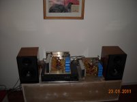
My current amp is an old NAD 3240 PE, which I've had for ages, and I was very curious to hear how the Crescendo's would sound in comparison.
I hooked up one channel in each chassis to the RCA-input contact, and set it up with an old NAD 1000 pre-amp and my CD player.
I retained the old speaker cables, 3m lengths of standard 4mm2 speaker cables, so as to get a prpoer comparison.
The first thing I noticed, was the power available. It didn't take much of a nudge on the volume controll before the speakers were pumping out music at rather impressive volume.
And the sound compared to the trusty old NAD?
Tighter. Especially the lower frequencies were reproduced in a much tigher and drier way.
generally, the music was better resolved and more detailed.
Cranking up the volume, reproduction remained completely unstrained and effortless, the limiting factor is overloading room-acoustics and my ears dynamic range.
Anything beyond this description would become subjective beyond making any sense.
The conclusion is that I'm extremely pleased with the result so far, this sounds like Hi-Fi.
I have not heard any of the other DIY designs out there, so I' can't say if you should build the Crescendo ME or any of the other DIY amps (many of which will allso undoubtedly be very good) our there.
What I can say is that if you expect to take the step from consumer audio up to "real" hi-fi reproduction, you will not be dissapointed.
The speakers are running improvised passive X-over, with no baffle step or equalisation of the DXT tweeter, so If I can get the x-over and equalisation right in the active crossovers, I expect great things.
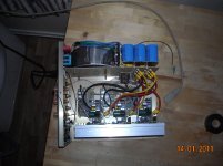
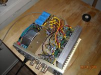
As you will see from the attached pictures, the amps are of a very compact design with a big 600VA toroid.
Due to this, I've been a bit aprehensive about possible hum problems.
If I put my ear up close to the speaker, I can hear a faint hum, the physical hum from the toroids is actually louder than this, so no big deal.
BUT.. the toroid in one chassis is hymming slightly louder than in the one in the other chassis, and the hum in the speaker connected to this cahssis is allso a bit louder. I wonder why this could be?
I will probably try to rotate the toroid a bit to see if that helps.
Anyway, just wanted to freshen up the thread a bit with some actuall results and listening impressions so far! 🙂
I have now fixed, tested and installed all six amplifier cards in their respective chassis.
I have yet to buuild and install the 3-way active x-overs going in to each chassis, so as such, the project is far from completed.
So far, this thread has dealt with various problems I've had to deal with for these Crescendo Milennium amps, both unexpected ones and damage caused by my own misstakes.
But what does these amplifiers sound like??
My current amp is an old NAD 3240 PE, which I've had for ages, and I was very curious to hear how the Crescendo's would sound in comparison.
I hooked up one channel in each chassis to the RCA-input contact, and set it up with an old NAD 1000 pre-amp and my CD player.
I retained the old speaker cables, 3m lengths of standard 4mm2 speaker cables, so as to get a prpoer comparison.
The first thing I noticed, was the power available. It didn't take much of a nudge on the volume controll before the speakers were pumping out music at rather impressive volume.
And the sound compared to the trusty old NAD?
Tighter. Especially the lower frequencies were reproduced in a much tigher and drier way.
generally, the music was better resolved and more detailed.
Cranking up the volume, reproduction remained completely unstrained and effortless, the limiting factor is overloading room-acoustics and my ears dynamic range.
Anything beyond this description would become subjective beyond making any sense.
The conclusion is that I'm extremely pleased with the result so far, this sounds like Hi-Fi.
I have not heard any of the other DIY designs out there, so I' can't say if you should build the Crescendo ME or any of the other DIY amps (many of which will allso undoubtedly be very good) our there.
What I can say is that if you expect to take the step from consumer audio up to "real" hi-fi reproduction, you will not be dissapointed.
The speakers are running improvised passive X-over, with no baffle step or equalisation of the DXT tweeter, so If I can get the x-over and equalisation right in the active crossovers, I expect great things.
As you will see from the attached pictures, the amps are of a very compact design with a big 600VA toroid.
Due to this, I've been a bit aprehensive about possible hum problems.
If I put my ear up close to the speaker, I can hear a faint hum, the physical hum from the toroids is actually louder than this, so no big deal.
BUT.. the toroid in one chassis is hymming slightly louder than in the one in the other chassis, and the hum in the speaker connected to this cahssis is allso a bit louder. I wonder why this could be?
I will probably try to rotate the toroid a bit to see if that helps.
Anyway, just wanted to freshen up the thread a bit with some actuall results and listening impressions so far! 🙂
Attachments
Very nice Elbert! congratulations on getting your amps up and running. This clearly has been a long road, but finally, you have the results!
😎
😎
A very long road in deed Bonsai!
And again, thank you for your help and support along the way! 🙂
It is in deed satisfying to finally hear some music comming out from this.
Now I'll see if I can improve the humming in the speakers a bit...
And again, thank you for your help and support along the way! 🙂
It is in deed satisfying to finally hear some music comming out from this.
Now I'll see if I can improve the humming in the speakers a bit...
Some problems ARE simple to solve... and in such cases, the problem is often that one fear the worst and start in the wrong end.
When I switched off the pre-amp with the power amps still on, the hum in the right speaker dropped to the same very low level as in the left one.
so the conclusion is that the hum didn't originate from the amp it self, probably came from the power supply in the nearby pre-amp. I assume that since I haven't fitted the front plate and the cover yet, this leaves the amplifiers more exposed to texternal EM disturbances.
- Status
- Not open for further replies.
- Home
- Amplifiers
- Solid State
- Crescendo Millennium offset problem