This current has to flow through the two emitter resistors on alternate half cycles, so we need to apply a 50% duty cycle.
Pdis = Iac^2 * 0r33 * 50% = 3.5355*3.5355*0.33*0.5 = 2.06W
This is only true, if You apply square wave. The rms current will be 1/PI*Iacp=1/3,14*5A=1,6A, with sine wave. This gives 0.85W dissipation...
Sajti
I cannot see why you have adopted your formula to predict the dissipation in the emitter resistor.
As far as I can see the emitter resistor current from a ClassAB switching output stage is the speaker current.
If the speaker current is known, then the emitter resistor current is the same value. Only the small amount of current passing into the NFB deducts from this.
The difference between a resistor in the speaker output lead and the two resistors in the upper and lower half of the switching stage is that the emitter resistor passes that current for a half cycle.
the power dissipated is half the of what a full waveform @ 100% duty cycle would dissipate.
I cannot see why you have adopted your formula to predict the dissipation in the emitter resistor.
I calculated same way, as the current consumption calculated in class B amplifier (bias current neglected). My idea is that the emitter resistors passing same current as the amplifier get from one power rail. Simple rms calculation is no applicable for this.
Sajti
Last edited:
hi Michael , can you please provide the entire schematic or at-least tell the name of the product ...
Regards
It's a Nakamichi PA7
Attachments
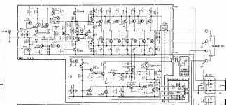
Wow, strange! What do the transistors Q102, Q103 actually do here?
Best regards!
They are working as zener diodes.
Sajti
Thanks, Sajti 🙂! As Zeners of about the BE breakdown voltage, i.e. about 6 to 7 volts, I presume?
Best regards!
Addendum: Still don't catch it. As the inverse polarized BE diode has been seen as a noise generator in some old designs, we might also observe some noise here?
Best regards!
Addendum: Still don't catch it. As the inverse polarized BE diode has been seen as a noise generator in some old designs, we might also observe some noise here?
Last edited:
Thanks, Sajti 🙂! As Zeners of about the BE breakdown voltage, i.e. about 6 to 7 volts, I presume?
Yes.
Sajti
Can SMD resistor 2512 package be used for current sharing purpose , I have used four 1E resistor in parallel to form the 0.25E in the emitter. does SMD resistors fails in long term usage in high temp situation ??? Mostly people used ceramic encased wire wound resistor for this type of application , is it only for cost reasons or due to the higher pulse power rating of them ....and aint the Wire wound resistors inductive in nature.. I have also noticed in high power amps when you do sine wave testing the resistors start producing a audible noise i.e the wire wound resistors start vibrating at the frequency of the test frequency ...
As the inverse polarized BE diode has been seen as a noise generator in some old designs, we might also observe some noise here?
Same for zeners. They are noisy.
Sajti
Same for zeners. They are noisy.
That's for sure. Maybe the transistor 'Zeners' are less noisy, so they decided to use them instead?
Best regards!
Sekhar, 2512 resistors can be used in parallel - for example, we have used 5 x 1 ohm resistors for achieving 0.2 ohm @ 5W in one of the early NS OPS based designs, however, after some time we have switched back to the cement 5W resistors, mostly because of the ease of servicing reasons. In case if some issues, it's much easier to replace one cement resistor, than five SMD ones.
hi,
any idea why am i getting the notch in lower half cycle when the amp goes into clipping ... I currently have the amp set up exactly as P3A ...??
any idea why am i getting the notch in lower half cycle when the amp goes into clipping ... I currently have the amp set up exactly as P3A ...??
Overdrive of output due to bootstrap. Post a picture, it's probably normal for this design.
Is this common for bootstrapped amplifiers.. and this notch starts happening after 4khz or so as i get the amp near to clipping
Attachments

In this case it might be insufficient drive current sourced from the bootstrap, if it was sufficient the positive rail should clip first. check the voltage of the bootstrap capacitor (between the two resistors).
You might need to run more current through the bootstrap (would not be surprising if you are using the 2 pair ops) or something else could be wrong with the components.
You might need to run more current through the bootstrap (would not be surprising if you are using the 2 pair ops) or something else could be wrong with the components.
In this case it might be insufficient drive current sourced from the bootstrap, if it was sufficient the positive rail should clip first. check the voltage of the bootstrap capacitor (between the two resistors).
You might need to run more current through the bootstrap (would not be surprising if you are using the 2 pair ops) or something else could be wrong with the components.
i am using two pairs , but i have faced the same problem with one pair also.. might be I am using 45V rails and a 4E load.. what should be the voltage across R9 ..?? and how do i increase the bootstrap current
Attachments
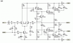
The differential voltage across R9 should be about 22V and steady across the audio range for 45V rails.
Before we proceed, can you measure DC coupled Vout on CH1 and the DC coupled voltage of the negative rail on the same scale on CH2.
Before we proceed, can you measure DC coupled Vout on CH1 and the DC coupled voltage of the negative rail on the same scale on CH2.
The differential voltage across R9 should be about 22V and steady across the audio range for 45V rails.
Before we proceed, can you measure DC coupled Vout on CH1 and the DC coupled voltage of the negative rail on the same scale on CH2.
Yes I will measure and post the data... Tonight do I need to measure the DC voltage on load or no load
Thank you
A bootstrapped VAS supply will clip on signal going towards one rail. That rail will depend on which VAS one has chosen. It is not always the +ve side that gets clipped first.In this case it might be insufficient drive current sourced from the bootstrap, if it was sufficient the positive rail should clip first. check the voltage of the bootstrap capacitor (between the two resistors).
You might need to run more current through the bootstrap (would not be surprising if you are using the 2 pair ops) or something else could be wrong with the components.
- Status
- Not open for further replies.
- Home
- Amplifiers
- Solid State
- Correct location for VBE bias transistor on CFP output amplifier