Workhorse said:Superb Evita!!!
One question....
Why you have used seperate groung planes in this daughterboard [seperate logic and analogue G-planes if i am correct]and even on the motherboard containing amp+smps......Why not single one??[I think i am missing something]
Is it for isolating the smps primary ground from amp ground......
Like in UCD [hypex] they are also using single breakfree ground plane on the top.....
The separate ground planes in the motherboard reflect the galvanic isolation between the battery ground and the audio ground.
The analog and digital ground planes are split and joint in a single point because I'm using the analog one as a signal ground reference in several places and I don't want "mixed signal ground loops". The TDA7318 has a digital ground pin for that purpose too. I don't want to "hear" display and I2C series communication signals.
This is a quick project, particularly the preamp board that was designed and built within 3 days, but there is still some quality in it... 😀😀😀
Some pictures of the preamp board assembled and working...

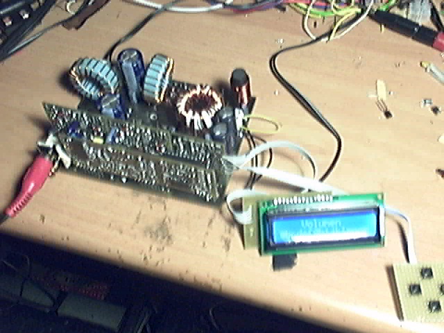

The I2C communication with the TDA7318 seems to work, including ACK checking. I adapted some code that I wrote some time ago to interface with I2C EEPROMS. There is nothing to read from this IC which makes things much easier.
The communication with the HD44780-compatible display is now working too (this is the first time I use a display). It employs a 3-wire to 11-wire interface board that is mounted behind it (write-only). I got the 3 wire idea here: http://home.iae.nl/users/pouweha/lcd/lcd_examp.shtml (my circuit is a mix of the two solutions proposed). This blue display looks really nice, particularly if we consider how much I paid for it in ebay 😀😀😀 Optimum LCD bias voltage seems to be 1V.
There is still some simple "human interface" code to write...
Evita,You are creating a havoc on the forum!!!!
What are the 4 keypads for......2 for volume and 2 for??
What are the 4 keypads for......2 for volume and 2 for??
Workhorse said:Evita,You are creating a havoc on the forum!!!!
What are the 4 keypads for......2 for volume and 2 for??
4 for menu browsing, as usual.
The interface has to be minimal because adding weather-proof keyboards and displays to a motorbike is not easy. Control keys are up, down, function and mute, but the mute key may disappear. The display may also just disappear or be replaced by one half the size (8x2). I just wanted to test these blue displays (I have 16x2 and 20x4).
BTW: Info on sources or DIY ideas for 3-key or 4-key weather-proof keyboards is welcome 😉
BTW: Info on sources or DIY ideas for 3-key or 4-key weather-proof keyboards is welcome 😉
Eva said:BTW: Info on sources or DIY ideas for 3-key or 4-key weather-proof keyboards is welcome 😉
try IR optical.
djQUAN said:how much would an amp like that cost? I want one! 😀
I don't really know, this is only a first DIY-style prototype that has yet to be further tested and improved. Please be patient. Once this prototype is finished and mounted in the motorbike we may discuss about the next prototypes, but please do it through private mail.
eva 🙂
perhaps i 'll said some thing to make you unhappy
but i like to say something about ur project
because i like your words:
I use to feel like the small child in The Emperor's New Clothes tale
ur pcb design is not good as ur thinking when u was designing it .
1st:
the gate charge line is toooo long.
this will make the inductor of g pin too large.
so ringing and slowly.
i've never put the driver of mosfet so faraway from the mosfet.
i think mini-loop design is very important at class-d project.
2nd:
ur power supply line (from Diodes to mosfet) is not good for two channel working together.
not enougth Separate,
i think two Separate lines to two channels will be better.
post a pic about my mosfet driver,
250w rms to 4ohm
(dont ask for the another sideof pcb)
not to care about the feeling of my words,
because i dont know what feeling will be cause from my words
i'v never living outside china.
sorry for my poor english.
rg
fumac
🙂
Attachments
Hi Fumac
First of all, note that this is my very first class D audio amplifier. I have developed other class D prototypes during the last 18 months but neither of them was intended to amplify audio (I started to flirt with class D on May 2006).
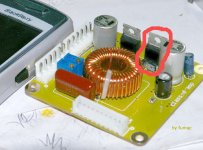
Indeed, there are some pitfalls in the layout that have become evident during testing, but none of them was particularly disastrous. The PCBs shown are perfectly useable.
The point about long gate drive tracks is very well taken, but I don't use gate resistors as everybody is doing, I use only ferrite beads and they are 20 times more inductive than those long PCB tracks, thus yielding track parasitistics negligible.
I don't understand what you explain about the power supply lines. RF voltage drop across wide PCB polygons with a ground plane on the opposite side is negligible, all the HF voltage ripple seen on the supply rails comes from the resistive nature of the electrolytic and ceramic capacitors employed. Since the capacitors are shared, the only way to isolate each channel from the supply ripple of the other is to use separate capacitors for each channel fed by separate pi filters, but I don't have place for that. Note that your circuit seems to lack something very important: PI filters to prevent RF to escape through supply wiring. My circuit doesn't need this because the leakage inductance of the transformer already does a very good job preventing ripple from reaching the 12V input.
I have not posted for the past few days because I have been busy writing the firmware and doing other things. The firmware is written in assembler, fills a PIC16F84A completely and it does some useful things:
- It allows to change volume, bass, trebble, and balance and the settings are stored in EEPROM when it detects that you are turning the amplifier off. They are recalled upon next power up.
- It does delayed startup (for supressing TDA7318 single-supply thump), it implements a mute function key with adjustable mute volume and it always ramps volume in a smooth way to avoid pops.
- It implements a configuration mode where the you can adjust turn-on volume (or disable it), mute volume, input gain 0/6/12/18dB, and it also allows to change the welcome and title message that is displayed on power up and after a few seconds without pressing any button.
I have been also improving gate drive. First I reduced the dead time on high-side to low-side switching transitions to below what my eyes can see on my CRT oscilloscope at 50ns/div (I think there is 5ns error or less).
Then, I found a very strange behaviour on the low-side to high-side switching transients: I was getting up to 30ns dead time that was dependent on the bass content of the music signal and it could not be cancelled by tweaking gate charge/discharge speeds, even with strong overlapping and cross-conduction this strange dead time was still there.
I investigated further and found that the propagation delay from the output of the comparator to the low-side gate was very constant with no visible jitter, both for turn-on and turn-off, but the propagation delay to the high-side gate was not constant, it seemed to suffer from up to 30ns of signal-dependent jitter!!
This strange behaviour made me think a lot. At first I blamed the IR2010 gate driver, but then other idea came to my mind: MOSFET switching times are completely dependent on gate driver supply voltages!!!
In fact, the low side gate driver is fed by a 18V regulator, but the high side driver is fed by the bootstrap system, where the diode, the series resistor and the capacitor don't have zero impedance and are subject to wide changing peak to average current ratios that result in audio-signal-dependent voltage drops. So first I tried shorting the 22 ohm resistor that I had in series with the bootstrap diode and it resulted in a 50% reduction in the strange bass-dependent jitter. Then, I paralleled a 100uF bootstrap capacitor to the existing 4.7uF one and as a result all the jitter disappeared. Finally, I tried removing the jumper across the previously mentioned 22 ohm resistor and the jitter was still absent.
Now, dead time is below 3ns in both directions 😀😀😀 So it may be time for measuring THD...
First of all, note that this is my very first class D audio amplifier. I have developed other class D prototypes during the last 18 months but neither of them was intended to amplify audio (I started to flirt with class D on May 2006).
Indeed, there are some pitfalls in the layout that have become evident during testing, but none of them was particularly disastrous. The PCBs shown are perfectly useable.
The point about long gate drive tracks is very well taken, but I don't use gate resistors as everybody is doing, I use only ferrite beads and they are 20 times more inductive than those long PCB tracks, thus yielding track parasitistics negligible.
I don't understand what you explain about the power supply lines. RF voltage drop across wide PCB polygons with a ground plane on the opposite side is negligible, all the HF voltage ripple seen on the supply rails comes from the resistive nature of the electrolytic and ceramic capacitors employed. Since the capacitors are shared, the only way to isolate each channel from the supply ripple of the other is to use separate capacitors for each channel fed by separate pi filters, but I don't have place for that. Note that your circuit seems to lack something very important: PI filters to prevent RF to escape through supply wiring. My circuit doesn't need this because the leakage inductance of the transformer already does a very good job preventing ripple from reaching the 12V input.
I have not posted for the past few days because I have been busy writing the firmware and doing other things. The firmware is written in assembler, fills a PIC16F84A completely and it does some useful things:
- It allows to change volume, bass, trebble, and balance and the settings are stored in EEPROM when it detects that you are turning the amplifier off. They are recalled upon next power up.
- It does delayed startup (for supressing TDA7318 single-supply thump), it implements a mute function key with adjustable mute volume and it always ramps volume in a smooth way to avoid pops.
- It implements a configuration mode where the you can adjust turn-on volume (or disable it), mute volume, input gain 0/6/12/18dB, and it also allows to change the welcome and title message that is displayed on power up and after a few seconds without pressing any button.
I have been also improving gate drive. First I reduced the dead time on high-side to low-side switching transitions to below what my eyes can see on my CRT oscilloscope at 50ns/div (I think there is 5ns error or less).
Then, I found a very strange behaviour on the low-side to high-side switching transients: I was getting up to 30ns dead time that was dependent on the bass content of the music signal and it could not be cancelled by tweaking gate charge/discharge speeds, even with strong overlapping and cross-conduction this strange dead time was still there.
I investigated further and found that the propagation delay from the output of the comparator to the low-side gate was very constant with no visible jitter, both for turn-on and turn-off, but the propagation delay to the high-side gate was not constant, it seemed to suffer from up to 30ns of signal-dependent jitter!!
This strange behaviour made me think a lot. At first I blamed the IR2010 gate driver, but then other idea came to my mind: MOSFET switching times are completely dependent on gate driver supply voltages!!!
In fact, the low side gate driver is fed by a 18V regulator, but the high side driver is fed by the bootstrap system, where the diode, the series resistor and the capacitor don't have zero impedance and are subject to wide changing peak to average current ratios that result in audio-signal-dependent voltage drops. So first I tried shorting the 22 ohm resistor that I had in series with the bootstrap diode and it resulted in a 50% reduction in the strange bass-dependent jitter. Then, I paralleled a 100uF bootstrap capacitor to the existing 4.7uF one and as a result all the jitter disappeared. Finally, I tried removing the jumper across the previously mentioned 22 ohm resistor and the jitter was still absent.
Now, dead time is below 3ns in both directions 😀😀😀 So it may be time for measuring THD...
Old waveforms showing 50ns jitter in power stage toggling during loud music playback. This is the usual behaviour of most class D stuff out there. The dead time concept was inherited from SMPS where efficiency prevaiuls over linearity.
High side to low side:
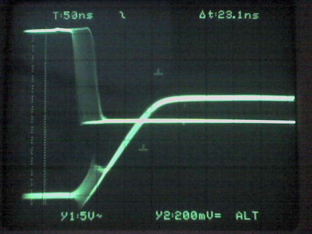
Low side to high side:

New waveforms with hard to see jitter during loud music playback:
High side to low side:

Low side to high side:

All measurements WRT comparator output.
High side to low side:
Low side to high side:
New waveforms with hard to see jitter during loud music playback:
High side to low side:
Low side to high side:
All measurements WRT comparator output.
Eva said:Then, I paralleled a 100uF bootstrap capacitor to the existing 4.7uF one and as a result all the jitter disappeared.
Evita, finally you gave up on using tiny cap for high side bootstrap......Bass Transients provoke these actions!!!!
Thats why i like active solution to power up high side driver all the time
safe with all types of dutycycles 0-100%
😀 😀 😉
Very nice. That's a perfect fit to my findings in the IRS20954 thread that the switching behavior is strongly depending on the supply of the drivers. In the set up which I had that time I found even much more than 30ns....
This was one of the multiple reasons why I am investing the efforts for a dedicated synchronized on board flyback with regulation and 100uF caps for all the needed auxiliary supplies in my Gen2.
This was one of the multiple reasons why I am investing the efforts for a dedicated synchronized on board flyback with regulation and 100uF caps for all the needed auxiliary supplies in my Gen2.
ChocoHolic said:This was one of the multiple reasons why I am investing the efforts for a dedicated synchronized on board flyback with regulation and 100uF caps for all the needed auxiliary supplies in my Gen2.
Choco also like active gatedrive supplies......🙂
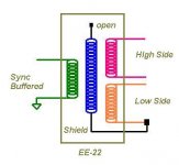
below is the gate driver supply transformer configuration of a professional company 8KW Class-D.....There is a special shield connected to lower side rail, i think its purpose is to eliminate capacitive coupling between secondary and primary windings......
Attachments
I will continue using tiny bootstrap capacitors for SMPS because they are perfectly fine if you don't mind some jitter (which is very advantageous in SMPS because it results in lower EMI due to a spread spectrum).
Separate supplies are a big no-no, they bring plenty of new problems. The amount of components and circuit traces attached to the switching node should be kept to an absolute minimum due to capacitive coupling to modulators and analog input stages, failing to met this criteria results in increased cross-talk and THD, not to mention the order of complexity of the resulting parasitistic RLC systems at RF. Transformers? No, thanks, I'm busy enough dealing with MOSFET package parasitistics 😉
Separate supplies are a big no-no, they bring plenty of new problems. The amount of components and circuit traces attached to the switching node should be kept to an absolute minimum due to capacitive coupling to modulators and analog input stages, failing to met this criteria results in increased cross-talk and THD, not to mention the order of complexity of the resulting parasitistic RLC systems at RF. Transformers? No, thanks, I'm busy enough dealing with MOSFET package parasitistics 😉
Speaking of transformer for driving mosfet gates, I'm about to experiment with PulseEng B2136 for driving high and low mosfets. The windings seems to fit Kanwar's post#98, but without center winding. Origiinally this is of ADSL drive transformer.
What do you think, is this transformer can be used for such purpose? (fosc=400khz)
What do you think, is this transformer can be used for such purpose? (fosc=400khz)
- Status
- Not open for further replies.
- Home
- Amplifiers
- Class D
- Cool and small 2x150W class D full-range car amplifier