I LOVE ceramic SMD chip capacitors!!!!!! They can avoid a lot of EMI when you put them in the right place...
Crosstalk improved by another 12dB or so.
When the amplifier is idle, channels no longer run synchronized due to parasitistics. Now they are 30Khz apart and I have to touch with my fingers some critical circuit node in order to cause them to synchronize due to parasitistic crosstalk (as they were before).
Now, when one channel is driven and the other channel is idle, you can only hear an increased noise floor in the idle channel, it's barely audible.
Photonicube said:Hey Eva, your project is look very nice. Have you played around with IRF's Direct Fets at all, I am currently working on a design using the IRF6662. You can get an amazing amount of current through them for their physical sizes.
I don't like directfets. It's been said that the new amplifiers built around them (Alpine for example) are all failing. BGA style packages were never intended for power applications. Furthermore, it seems that these packages don't eliminate parasitistics, they just shift them up in frequency making them more troublesome to detect and control but much more likely to be radiated. I like TO-220.
BTW: How do you replace a blown directfet? (How much does it cost the required soldering equipment?)
Eva said:
BTW: How do you replace a blown directfet? (How much does it cost the required soldering equipment?)
I haven't worked with directfets but 98% of SMD components can be removed with a good hot air rework station and I would think directfets are no exception.
😀
to replace a blown fet, a smd hot air rework gun is needed. you can find cheaper ones around $170, like this one: http://www.mpja.com/prodinfo.asp?number=15143+TL
As for the blown fets themselves, it has been my experience, that they are a little more delicate than a equivalent part in say a TO-220 package. The main cause of Direct fet's failing in my designs has been due to me treating them like a TO-220, I have found that the package it's self can't take avalanche energy very well (even more so than stated in the data sheet) nor can the body diode handle clamping flyback energy from the main inductor very well. As such, once I learned how to deal with the parts, and protect against their frailties, they became rather useful. I too like the TO-220 parts better when the space permits, but some times my job requires me to cram more power into smaller spaces.
As for the blown fets themselves, it has been my experience, that they are a little more delicate than a equivalent part in say a TO-220 package. The main cause of Direct fet's failing in my designs has been due to me treating them like a TO-220, I have found that the package it's self can't take avalanche energy very well (even more so than stated in the data sheet) nor can the body diode handle clamping flyback energy from the main inductor very well. As such, once I learned how to deal with the parts, and protect against their frailties, they became rather useful. I too like the TO-220 parts better when the space permits, but some times my job requires me to cram more power into smaller spaces.
Even with hot air, I still don't understand how one can manage to heat the small solder contacts *under* the package to 250ºC for proper solder melting without overheating everything around the transistor (or the own transistor), or causing the parts near the transistor to desolder first, or heating the entire board and components to 260ºC as in industrial manufacturing.
Do you mean that you have seen directfets failing in class D because of too hard switching? This may have to do with the 7.5nH leakage inductance that every TO-220 MOSFET has in its drain terminal because it helps in limiting di/dt nicely (although most people don't think about this). Also, less avalanche tolerance is to be expected from a package with the die attached to a much smaller thermal pad and thus much less transient thermal capabilities.
BTW: I hope that IR continues making new parts in TO-220 packages because the die inside a IRF6662 seems to be quite improved over, say, the IRF540Z that I use. Gate charge is much lower, Rds-on is slightly lower and body diode is equally fast.
Since the metal can is connected directly to the die it's self heat transfers pretty well through the part and into the solder points, a low air flow is needed to keep the other components around the fet from being removed.
Yes, that is what I have speculating as a possible failer cause, I have noticed that longer trace lengths to the drain and source of the fets does seem to help them last longer (but really hurts EMI). I think the high dI/dT is causing high instantaneous heating leading to the eventual death of the part. Maybe I'll try a 7nH inductor really close to fet and see how that effects it in a know failer circuit.
Yes, that is what I have speculating as a possible failer cause, I have noticed that longer trace lengths to the drain and source of the fets does seem to help them last longer (but really hurts EMI). I think the high dI/dT is causing high instantaneous heating leading to the eventual death of the part. Maybe I'll try a 7nH inductor really close to fet and see how that effects it in a know failer circuit.
Those 7nH are not drain inductance, but *source* inductance. Sorry for the mistake. Source inductance appears effectively in series with gate drive voltage and its effects are seen as false spikes in Vgs at turn-on before the "flat" portion (I suppose you know what I'm talking about). A 3V to 4V spike in a TO-220 means di/dt is in the 500A/us range. I think that those spikes reduce instantaneous gate drive and produce a di/dt limiting effect.
A piece of thin PCB track may do the inductance trick, it's just a matter of not grounding the gate drive circuit exactly at the source terminal and leaving some inductive shared path for gate drive and source current.
A piece of thin PCB track may do the inductance trick, it's just a matter of not grounding the gate drive circuit exactly at the source terminal and leaving some inductive shared path for gate drive and source current.
Hey, this is a nice one too 😉 but the extra current capability comes at the expense of extra output capacitance and extra losses,. It employs definitely a bigger die than IRF540Z. I use to buy the stuff for my prototypes from farnell and 25 pieces of each of these two devices cost the same there. I'll give them a try if I need higher current capability.
More on self oscillating class-D crosstalk
The previous crosstalk tests were done with the offending channel unloaded. Now I have tried connecting a 11.2 ohm dummy load to the offending channel and to my surprise I got another 12dB or so of improvement in crosstalk and the spectrum is now much more white-noise like without any traces of the original music signal.
Indeed phase-shifted self-oscillating has quite unexpected features and in my opinion it is a big step ahead of triangle wave modulation.
Re: More on self oscillating class-D crosstalk
You envy sync!!!😉
Eva said:Indeed phase-shifted self-oscillating has quite unexpected features and in my opinion it is a big step ahead of triangle wave modulation.
You envy sync!!!😉
Too fast gate drive at turn-off.
I feel stupid because at turn-off I have measured 1.3V and 1.8V spikes respectively across the PCB tracks that connect MOSFET sources with the corresponding pins of IR2010. I can see clearly how the voltage grows if I move the probe tip across the PCB track. Also, these spikes are so narrow that their amplitude is probably 50% higher than measured because they are outside the bandwidth of my oscilloscope.
This shouldn't be a problem, but it is because I'm referencing stuff to the low-side source tracks and I don't want it floating that much in common mode, and because I run output feedback tracks near one of the gate tracks that is also suffering similar inductive voltage drops and the feedback tracks are picking up spikes due to coupling.
This is definitely calling for a slow down in turn-off speed (and for an improved layout next time).
Pictures of switching behaviour
I managed to take some pictures of switching behaviour. They show the false peak in Vgs due to opposite side body diode reverse recovery (just before the Vgs plateau stage) and the dead time in both directions. They were taken while playing loud music with the oscilloscope in analog mode to allow for 50ns/div timeresolution and in order to get a "sprayed" image of all the switching behaviours the circuit can exhibit depending on input signal. CH1 probe is 1x and shows Vgs while CH2 probe is 100x and shows Vds (I'm short on probes.) I took sync in advance at the output of the LM311 in order to show the beginning of the waveforms properly.
Note the nice turn-on Vgs ramp produced by the big ferrite beads, and the complete absence of ringing.
BTW: I still have to get rid of all this ugly dead time...
Turn-on:
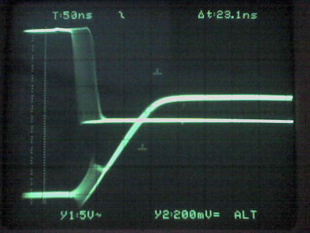
Turn-off:

I managed to take some pictures of switching behaviour. They show the false peak in Vgs due to opposite side body diode reverse recovery (just before the Vgs plateau stage) and the dead time in both directions. They were taken while playing loud music with the oscilloscope in analog mode to allow for 50ns/div timeresolution and in order to get a "sprayed" image of all the switching behaviours the circuit can exhibit depending on input signal. CH1 probe is 1x and shows Vgs while CH2 probe is 100x and shows Vds (I'm short on probes.) I took sync in advance at the output of the LM311 in order to show the beginning of the waveforms properly.
Note the nice turn-on Vgs ramp produced by the big ferrite beads, and the complete absence of ringing.
BTW: I still have to get rid of all this ugly dead time...
Turn-on:
Turn-off:
Preamplifier board almost ready to assemble.

Inputs are balanced (U1 is TL074). This first prototype includes a TDA7318 IC that I got from an old car radio to provide volume, balance, bass and trebble controls because this amplifier has to work alone and being fed only by the line-out of an I-pod (remember that it will be used in a motorbike).
It also includes a LM339 comparator that provides DC detection on the outputs, and a PIC16F84 to send the I2C signals to the TDA7318, read the 4 control keys and send information to an optional display (I got some low-cost Chinese displays that I want to test).
The L4916 and L4949D voltage regulators that provide 8.5V for the TDA7318 and 5V and reset signals from the PIC were also taken from the same old car radio 😀😀😀
Eva said:I'm insane and you like it? Thanks 😀 Messages like yours are a good source of motivation. Of course I'm always open to business 😀 I'll try to mail you, otherwise mail me or contact me through messenger (see my forum profile)
Thanks, Eva. I will try to write you over the weekend (USA Thanksgiving holiday). After I stuff myself silly with food, I'll have nothing better to do than talk audio. 😀
"(remember that it will be used in a motorbike)."
I was debating between the 41 hertz amp 32 and the Nolan N-102 with N-Comm.
Now I'm watching this thread. 😀
I was debating between the 41 hertz amp 32 and the Nolan N-102 with N-Comm.
Now I'm watching this thread. 😀
I did a google search about the Nolan N-102 just for curiosity and found out that it's a helmet with built-in intercom, quite interesting... Then and I continued searching and I ended up reading opinions about it in some Spanish motorbike forums: It's a really noisy helmet, people that bought it doesn't seem to recommend it at all 😀😀😀
BTW: Your choice depends a lot on how big are the speakers that you want to power and how much space do you have. My amplifier is much bigger than AMP-32, the PCB measures 125mm width, 100mm depth and 50mm height (including a simple aluminium plate heatsink). However, it's also much powerful, and this first prototype has a multi-function pre-amp board with remote volume and tone control (neither required nor desirable for car applications).
BTW: Your choice depends a lot on how big are the speakers that you want to power and how much space do you have. My amplifier is much bigger than AMP-32, the PCB measures 125mm width, 100mm depth and 50mm height (including a simple aluminium plate heatsink). However, it's also much powerful, and this first prototype has a multi-function pre-amp board with remote volume and tone control (neither required nor desirable for car applications).
Pre-amplifier board:


It fits nicely on the main board, even with the regulators still mounted on the top side. The SO SMD ICs were not that hard to solder, except because I used a standard SO20 package for the L4949DW which has a widebody profile. The 18 pin socket is going to have a PIF16F84A in it. Now it's time for some coding...
It fits nicely on the main board, even with the regulators still mounted on the top side. The SO SMD ICs were not that hard to solder, except because I used a standard SO20 package for the L4949DW which has a widebody profile. The 18 pin socket is going to have a PIF16F84A in it. Now it's time for some coding...
Superb Evita!!!
One question....
Why you have used seperate groung planes in this daughterboard [seperate logic and analogue G-planes if i am correct]and even on the motherboard containing amp+smps......Why not single one??[I think i am missing something]
Is it for isolating the smps primary ground from amp ground......
Like in UCD [hypex] they are also using single breakfree ground plane on the top.....
- Status
- Not open for further replies.
- Home
- Amplifiers
- Class D
- Cool and small 2x150W class D full-range car amplifier