Re: Incidentally...
An utterly confusing abuse of terminology.
mikeks said:...these designs look attractive, but alas, the beauty is purely visual....
An utterly confusing abuse of terminology.
Re: Parasound..
Hi Mike,
The Audio drive from Elektor (march 2005) uses the same topology as that parasound amp. I did simulations with that topo and used the Q107 - Q110 configuration as my second diff pair+VAS. Unfortunalety it didn't give me enough gain. And using this kind of topo instead of my VAS causes unstability (3 diff pairs after each other).
This ain't a folded cascode hé? Or do I understand you wrong.
Mike, do you maybe have a schematic like the one Bocka is explaining?
Greetz
Ben
mikeks said:...example in which the second stage's emitter is buffered from the first stage...(Q107 &Q109):
Hi Mike,
The Audio drive from Elektor (march 2005) uses the same topology as that parasound amp. I did simulations with that topo and used the Q107 - Q110 configuration as my second diff pair+VAS. Unfortunalety it didn't give me enough gain. And using this kind of topo instead of my VAS causes unstability (3 diff pairs after each other).
This ain't a folded cascode hé? Or do I understand you wrong.
Mike, do you maybe have a schematic like the one Bocka is explaining?
Greetz
Ben
Ben,
Maybe a partial showing the area of interest would be fine, which I believe is ok for instructive uses, the copy of the whole article is of course not allowed without permission.
Regards,
Jam
Maybe a partial showing the area of interest would be fine, which I believe is ok for instructive uses, the copy of the whole article is of course not allowed without permission.
Regards,
Jam
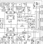
Hi,
any idea why the test voltages across R26 & R27 are different?
That's the first time I have noticed protection diodes across the inverting and non inverting inputs of a discrete amp. Just like some opamps! Are there any disadvantages in doing this?
any idea why the test voltages across R26 & R27 are different?
That's the first time I have noticed protection diodes across the inverting and non inverting inputs of a discrete amp. Just like some opamps! Are there any disadvantages in doing this?
Andrew,
The protection diodes are there to protect the diff pair dual transistors against to high emitter-base voltages. The max Vbe for these devices is 5V.
I can't explain wy the voltages over R26 and R27 would be different. For me, it looks like an error on the schematic.
Greetz
Ben
The protection diodes are there to protect the diff pair dual transistors against to high emitter-base voltages. The max Vbe for these devices is 5V.
I can't explain wy the voltages over R26 and R27 would be different. For me, it looks like an error on the schematic.
Greetz
Ben
Bensen said:Andrew,
The protection diodes are there to protect the diff pair dual transistors against to high emitter-base voltages. The max Vbe for these devices is 5V.
Greetz
Ben
No, something "else" will happen before "that" you interpreted wrong! 🙂
Cheers Michael
AndrewT-
Hi,
any idea why the test voltages across R26 & R27 are different?
ah youre a funny Guy, is because of component tolerance
mikeks-
...that looks like complexity for its own sake....
Hi Mike youre a funny Guy
Hi,
any idea why the test voltages across R26 & R27 are different?
ah youre a funny Guy, is because of component tolerance
mikeks-
...that looks like complexity for its own sake....
Hi Mike youre a funny Guy
Hi Mastertech,
re component tolerance;- all the other quoted test voltages match to all significant figures. This one is out by 3.3%. Component tolerance, I think not.
Which types of ClassA do you specialise in? SE, PP, Tube, FET, BJT, transformer coupled, etc?
re component tolerance;- all the other quoted test voltages match to all significant figures. This one is out by 3.3%. Component tolerance, I think not.
Which types of ClassA do you specialise in? SE, PP, Tube, FET, BJT, transformer coupled, etc?
Ultima Thule said:
No, something "else" will happen before "that" you interpreted wrong! 🙂
Cheers Michael
Ultima Thule,
Do you mean when the amp is clipping? Please, tell me.
mastertech said:AndrewT-
Hi,
any idea why the test voltages across R26 & R27 are different?
ah youre a funny Guy, is because of component tolerance
mikeks-
...that looks like complexity for its own sake....
Hi Mike youre a funny Guy
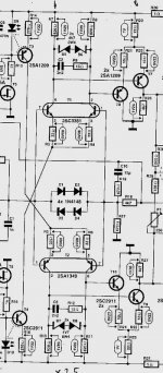
mastertech ,
I first thoucht that also, but the emitter currents are the same, so base current must be about the same also, if the Hfe of the 2SA1209 and 2SC2911 is the same (these are pretty good complementary devices). Or could it be that the base current of one of the PNP driver is bigger than this of the NPN driver (upper one). Than you have a point Mastertech.
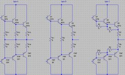
jam said:Ben,
What kind of output stage does it use...........a CFP?
Jam
Jam,
I don't know these terms good enough (CFP?). So I attached a picture. This amp uses type C as output arrangement. The only difference is that this amp uses 1 pair of drivers and no predrivers as in type C.
Attachments
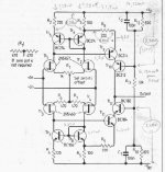
ANDREWT post 58
"I've looked at that JCurl 1981 schematic and I think it is a folded cascode."
MIKEKS post 60
"In fact, the second stage is an unbuffered differential stage..."
I consider that each VAS device of Curl's amp as being purely voltage driven by the voltage between the collectors of the input differential pair. I think there is no local feedback by the 10 Ohm emitter resistance. Am I right ?
~~~~ Forr
§§§
- Status
- Not open for further replies.
- Home
- Amplifiers
- Solid State
- Complementary diff input with JFET and BJT cascode