Yes, I bought Sprint 6.0 but I'm having trouble getting my head wrapped around it. I'm looking forward to learning it.
What part are you having trouble with? Many of us have used it. We can walk you through just about any part of it.
Hi Jeff,
I appreciate the offer. Jason has offered to help as well. I want to work at it a bit before I ask too many silly questions. I love the layouts guys make so I am encouraged about the possibilities.
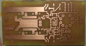
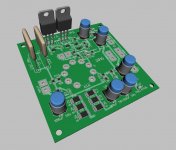
Meanwhile, I am trying my first attempt at a dual sided etching job. This should be interesting. There are no vias of course so I need to stay mindful of where they would be. Should be interesting. 😀
Blessings, Terry
I appreciate the offer. Jason has offered to help as well. I want to work at it a bit before I ask too many silly questions. I love the layouts guys make so I am encouraged about the possibilities.
Meanwhile, I am trying my first attempt at a dual sided etching job. This should be interesting. There are no vias of course so I need to stay mindful of where they would be. Should be interesting. 😀
Blessings, Terry
Attachments

Not meant as a critical comment .... But the double sided ground planed
OPS looks to increase the possibility of mishaps (bridges , more tracks).
Technically , for audio .... diminishing returns ( or none at all).
PS - for a OEM , the reduced copper to be etched would save on the
chemistry. And it does look pretty.
Not meant as criticism , just an objective observation. I DID research
planes/audio. Use can be good or bad , depending on layout / general
operating environment. A plane has lower L but higher C. What parts
of a circuit would benefit from less of either ?
The general consensus on the web is to apply the planes to where they matter
and not to where they will diminish the optimal.
Of course ,audio "planing" seems to fall into the same subjective discourse
as caps and exotic materials. 😀 (hard to find purely objective recommendations).
OS
Well I figure this will be a little tricky to solder without solder mask. I removed some of the screen to help reduce the chance of solder bridges but still the gaps between traces are tiny so should be fun. Time will tell if there is any issues with the large ground plane.
Last edited:
A generously compensated amp will not have any "issues". val's amps , my amps
could most likely be laid out with point to point wiring - all over the place ... and
still work.
My comment was just meant to point out the actual real world things that happen
with this choice (and traditional) layout styles. A few pF or picohenries won't
kill the bird !
OS
could most likely be laid out with point to point wiring - all over the place ... and
still work.
My comment was just meant to point out the actual real world things that happen
with this choice (and traditional) layout styles. A few pF or picohenries won't
kill the bird !
OS
Terry looks good! A high-quality etching  Well, in fact, for etching I can remove the plane - the ground connections are there anyway, they are just covered by the plane.
Pete - agree with every word. It definitely adds some picofarads/picohenries here and there, but at the same time - adds some "ground shield" effect. Well, my experinebts with CF-FET V2.0 (I've got both TH with no plane and SMD with a heavy plane) did not show any noticeable difference in stability, speed, square wave response performance. I hope, the one with the plane it's less sensitive to EMF inductance though (did not do any measurements yet)...
Well, in fact, for etching I can remove the plane - the ground connections are there anyway, they are just covered by the plane.Pete - agree with every word. It definitely adds some picofarads/picohenries here and there, but at the same time - adds some "ground shield" effect. Well, my experinebts with CF-FET V2.0 (I've got both TH with no plane and SMD with a heavy plane) did not show any noticeable difference in stability, speed, square wave response performance. I hope, the one with the plane it's less sensitive to EMF inductance though (did not do any measurements yet)...
yes , watch the output inductor. It would be interesting to actually see it's effect
in a parallel or perpendicular orientation to the plane ( or output track). PC
manufacturers generally go perpendicular to the plane (with a ferrite core).
One might think this is a non-event , but it is at many amps AC.
OS
in a parallel or perpendicular orientation to the plane ( or output track). PC
manufacturers generally go perpendicular to the plane (with a ferrite core).
One might think this is a non-event , but it is at many amps AC.
OS
Last edited:
yes , watch the output inductor. It would be interesting to actually see it's effect
in a parallel or perpendicular orientation to the plane ( or output track). PC
manufacturers generally go perpendicular to the plane (with a ferrite core).
One might think this is a non-event , but it is at many amps AC.
OS
From the measuring I did in my amp it looks like the inductor concentrates the fields out the ends. Another ray gun. Mounting it vertical might stop it from blasting towards the input depending on how the amp is layed out.
Hi Valery,
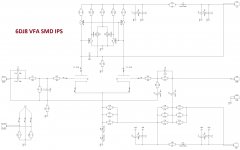
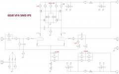
Did you think about doing an IPS version of this 6DJ8 circuit? I would be very interested in that.
Did you think about doing an IPS version of this 6DJ8 circuit? I would be very interested in that.
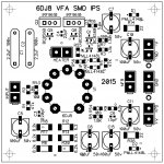
6DJ8 VFA SMD IPS
Here we go 🙂 I have dropped the ground plane here to ease the etching 😉
Cheers,
Valery
Hi Valery,
Did you think about doing an IPS version of this 6DJ8 circuit? I would be very interested in that.
Here we go 🙂 I have dropped the ground plane here to ease the etching 😉
Cheers,
Valery
Attachments
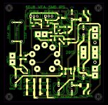
Good!!!Here we go 🙂 I have dropped the ground plane here to ease the etching 😉
Cheers,
Valery
Is it possible working this with 12au7?
Last edited:
The 12AU7 is a different pinout and a couple other values are different so it won't work.Good!!!
Is it possible working this with 12au7?
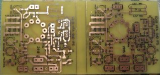
I am attaching a PDF for you if you want to do this IPS using photo etch.
Hi Valery,
I decided to go with the IPS so I etched and drilled a pair. I'm not sure if I have everything in stock so it may take a few days.
Blessings, Terry
Attachments


Hi Valery,
Is R12 a misprint? Why would you parallel a 6R2 with a bunch of 6K2's? It is that way on the schematic, silkscreen and BOM.
Thanks, Terry
Is R12 a misprint? Why would you parallel a 6R2 with a bunch of 6K2's? It is that way on the schematic, silkscreen and BOM.
Thanks, Terry
Terry, excellent example of double sided manual registration. 2x 6200 resistors in parallel with a
6R2 trim it down to 6R188.
Sent from my SM-N9005 using Tapatalk
6R2 trim it down to 6R188.
Sent from my SM-N9005 using Tapatalk
That is true but there are actually 5x6200ohm in parallel with one 6.2ohm. I'm not saying that the goal was not to achieve 6.1692ohm but it just looks suspicious.
Hi Terry,
Lightning-fast, as usual 🙂
Great quality etching / drilling
Sorry for a mistake - this is definitely a typo. All 6 resistors are 6.2K, it's just "K" is lost at one of the markings.
Cheers,
Valery
Lightning-fast, as usual 🙂
Great quality etching / drilling
Sorry for a mistake - this is definitely a typo. All 6 resistors are 6.2K, it's just "K" is lost at one of the markings.
Cheers,
Valery
Val
I would like to give a try to the #211 IPS but most of the resistors I do not have on the shelf 🙁
Please let me know If I can assemble the board with the values as bellow (gain is a bit differed too, but suits me OK).
What would be the VAS bias with 100R or 150R resistor ?
My supply i s2x 60V DC
Thanks
Peter
Attachments
Hi Peter,
I have checked your values - R3, R7 = 1.2K, R4 = 150R are fine (+/-60V rails).
6x5.6K result in VAS current = 15mA. Rather high, but acceptable with a decent heatsink.
Alert to everyone - found a typo mistake!
R7, R17, R18 must be 15K each!!!
Peter, in your case you can use 2x10K for the same value (5K), 2W is acceptable.
R8 = 1.5K, yes, slightly higher voltage gain (29.8db instead of 28.3db) - still OK.
Cheers,
Val
- Status
- Not open for further replies.
- Home
- Amplifiers
- Solid State
- "Compact" VFA