If you start going P2P style then yes there is some room for improvement but even Tomch places the Rfb on the PCB and does not have a shorter path than the chipamp.com version.
Yep
tomchr:
"The Influence of Circuit Layout on Stability
As noted in the LM3886 data sheet (p. 20), the inductance in the output lead of the amplifier IC greatly impacts stability. As a rule of thumb, figure that 1 mm of wire or PCB trace has a self-inductance of approx. 1 nH. Hence, the placement of the feedback resistor will have a big impact on amplifier performance.
The example below shows two common layouts of the LM3886 with resistive feedback. Only the feedback resistors have been included here. The dimensions marked in green are in mil (1 mil = 0.001″ = 25.4 µm).

...
As shown, the good layout results in approx. 240 mil (6.1 mm) of trace routing in the feedback network. Allowing for a little parasitic inductance in resistor R2, the parasitic inductance in the feedback path of the good layout is approx. 10 nH.
The poor layout exhibits 1.04″ (26.4 mm) of trace routing, resulting in a parasitic inductance of roughly 30 nH.
Simulations of the phase margin (PM) and gain margin (GM) were performed for a parasitic inductance, Lout, of 0 nH (ideal case), 10 nH (good layout), and 30 nH (poor layout). The results are plotted below (click for a larger view).
...

Note that the textbook definition of stability is that PM > 0 ° and GM < 0 dB. In an actual circuit, I prefer the PM to be greater than 60 ° and the GM below -10 dB.
The impact of the layout is pretty stark. Note how the poor layout (which really does not look that bad in the layout editor) causes the PM to fall off a cliff once the load capacitance exceeds 200 nF. The degradation in circuit stability is caused by the resonance of Lout and Cload. It’s pretty easy to spot the trouble brewing in the loop response. ... Note the resonance at 6.5 MHz. Once that peak crosses 0 dB, the circuit will oscillate. This is a tweeter eater."

from tomchr's:
LM3886 Chip Amp Stability Analysis
Last edited:
Yes,
I described that improvement last week to two Members. One changed his PSU layout to achieve low loop area.
It's all about the ROUTES that the Flow and Return currents have to follow.
post311.
Look at top right and bottom left.
Both have forced the Return current to follow a DIFFERENT Route from the Flow Current.
I think is so quiet you can't minimize loop area of grounding loop because the power wire of amplifer and pre made a big loop area out of them ? Is right ?
AudioLapdance, I was referring to the PCB design of the modulus-86 amp but the good example layout you posted is close to what chipamp.com is using. As far as I can remember Tomchr does not place Ri and Rfb parallel on his Modulus-86 design.
AudioLapdance, I was referring to the PCB design of the modulus-86 amp but the good example layout you posted is close to what chipamp.com is using. As far as I can remember Tomchr does not place Ri and Rfb parallel on his Modulus-86 design.
He started out like that:

But then moved it:

Because of the rest of his composite circuit:

I have TINA and tomchr's 3886 circuit. How would I model different loop areas rather than just trace lengths.

I guess you will only need to add a That1200, a servo, a composite opamp circuit and an excellent layout. Did I forget a good choice of the other parts?
Last edited:
Given that: "1 mm of wire or PCB trace has a self-inductance of approx. 1 nH."
Regarding fb resistors ...
There's close ... and then there's tomchr close :TM: !
and that's 1nH / mm regardless of trace width (does this apply to short pwr "planes"?)
Regarding hf ps caps ...
There's close ... and then there's tomchr close :TM: !
😉
Regarding fb resistors ...
There's close ... and then there's tomchr close :TM: !
and that's 1nH / mm regardless of trace width (does this apply to short pwr "planes"?)
Regarding hf ps caps ...
There's close ... and then there's tomchr close :TM: !
😉
Last edited:
Broadside Trace Inductance | Electronics and Electrical Engineering Tools | EEWeb Community
Here is an inductance toolbox. You can calculate for wire, loops and more. It is interesting to see how the inductance reduces when the return current is close.
Here is an inductance toolbox. You can calculate for wire, loops and more. It is interesting to see how the inductance reduces when the return current is close.
It's not a grounding loop that I am referring to.I think is so quiet you can't minimize loop area of grounding loop because the power wire of amplifer and pre made a big loop area out of them ? Is right ?
I said Flow route and Return route that currents have to follow.
There is close and there is extremely close.
I have placed the LM3886 on a heatsink and folded and soldered the resistor leads to the chip pins where they exit the package.
I have placed the LM3886 on a heatsink and folded and soldered the resistor leads to the chip pins where they exit the package.
Any idea what was the cause of that fail? I hope the tech wasn't badly injured.
No, the tech just received current in one hand. Luckily, he noticed the tingle and did not touch anything that could have completed a hard circuit. I guess his shoes were not fully insulating.
I pulled the brick out of service, but did not attempt an autopsy. It was a fully potted module, so it would have required some very nasty chemicals. It did have a bulge in the potting compound with cracks.
What it did do was highlight the fact that care must be taken with input voltage wiring, layout, and making sure all equipment has it's own safety bonding. All ground loop problems must never be fixed by the equivalent of a cheater cord.
It is interesting to see how the inductance reduces when the return current is close.
Terman's equation is great for calculating that.
jn
No, I was the one who said twist them in the first place.
You drew in the twisting of the power rails. And you kept it separate from the power ground, which is a terrible idea.
But I don't blame you for getting turned around, so many people have made up so many things and claimed I said them. Dunno what that's all about.
.
I only go by what you say and what you do. From your completely erroneous postings with regard to magnetic fields, it is clear to me that you do not understand the topic but use google searches to try and pull it off. If I had to guess, I'd say you are a high school student.
Attempting to use google to pretend understanding a complex topic never works on a forum where many posters have advanced degrees in E/M theory and/or physics, and have worked in those fields for decades. You are attempting to trash talk E/M theory with over 100 man years worth of experience...despite them trying to help you understand.
jn
Bent S,
If you google "hyperphysics", you'll find a really good site run by Georgia State University.
At their homepage, click on "electricity and magnetism", then "EMF", then "Faraday's law". It shows nicely how a ground loop acts when time varying magnetic fields are trapped by a loop.
Ampere's law shows how a wire creates a magnetic field.
Time varying current in the ground return wire will be trapped by the signal grounds if they are in close proximity, that is called mutual coupling.
If you google Tom Van Doren, you may find his presentation in ppt format, he goes into exactly what we've been trying to teach you.
jn
...
I have placed the LM3886 on a heatsink and folded and soldered the resistor leads to the chip pins where they exit the package.
Don't forget tomchr's work on point-to-point vs pcb:
http://www.diyaudio.com/forums/chip-amps/252436-lm3886-pcb-vs-point-point-data-34.html#post4127834
p-t-p is good for the fb res because it makes a shorter path but:
"To get the best performance out of the LM3886, you need to pay attention to the inductance of the ground nets. In particular, in the feedback and input ground reference. Use ground planes, properly."
tomchr:
http://www.diyaudio.com/forums/chip-amps/252436-lm3886-pcb-vs-point-point-data-34.html#post4128585
There is close and there is extremely close.
...
Speaking of which ...
"I got yer CLOSE for ya, right HERE!"


😉
(A better chipamp.com / BrianGT PCB ... but they still screwed-up the ps hf and mid freq (mf) bypassing. 🙄
Last edited:
There's no hard and fast rule, and it depends a lot on what amplifier the caps are supplying. The lower the cut-off, the better, but opamps have such good PSRR that they can live with much less decoupling than most discrete amps, for example. Usually the limitation is how much DC drop across the resistor you can live with. With opamps you see anything from 10 to 100 ohms, partnered with anything from 47u to 470u caps. This can give a cutoff anywhere from 338Hz which is 'better than nothing', to 3.38Hz, which is very good.I just have no idea what the value of R should be if my electros were say 220uF. My guess was that there is some kind of target frequency cutoff to locate the pole at to best stop any oscillation?
Bentsnake, you have gone from bad to worse. There are still several problems. For one, Vcc+ and Vee- are not a feed-and-return pair. Is it so difficult to do a current analysis?
Admirable intensity. But let's look at the facts.
<< Vcc+ and Vee- are not a feed-and-return pair >>
Sure they are. You can do the math if you like, or you can just look.
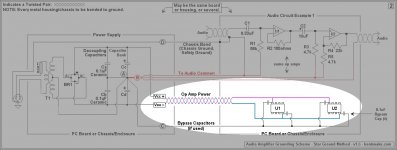
In the first image below apply E=IR. E is whatever the voltage might be, I is whatever the current flow might be.
R is the load, which is the op amps. Whether output (volume) is zero or non-zero, each op amp consumes perhaps 10ma--something--to operate. Circuit complete.
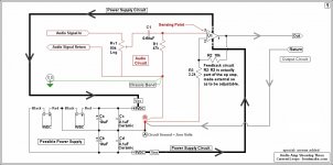
The second image clarifies this, I hope, but actually is mostly for fun. Note that here there are two complete (feed-and-return) circuits: The first circuit running the op amp, and a second circuit running an amp/speaker/headphone/whatever. The second circuit is a sub-circuit to the op amp, and has the indicated second return.
If anybody feels a need to do a circuit analysis for the zero-volume state, or for some other state, that's fine with me. But...why? Teams of engineers have already done this many times while they were creating the op amp in the first place. What point to reinventing the wheel?
The whole idea behind chip amps is that they're supposed to be easy. Those engineers have already done the heavy lifting, we just go along for the ride. What point there can be to making things hard, or especially to making things hard for somebody else, I cannot fathom.
.
Attachments
Admirable intensity. But let's look at the facts.
<< Vcc+ and Vee- are not a feed-and-return pair >>
Sure they are. You can do the math if you like, or you can just look.
In the first image below apply E=IR. E is whatever the voltage might be, I is whatever the current flow might be.
R is the load, which is the op amps. Whether output (volume) is zero or non-zero, each op amp consumes perhaps 10ma--something--to operate. Circuit complete.
The second image clarifies this, I hope, but actually is mostly for fun. Note that here there are two complete (feed-and-return) circuits: The first circuit running the op amp, and a second circuit running an amp/speaker/headphone/whatever. The second circuit is a sub-circuit to the op amp, and has the indicated second return.
If anybody feels a need to do a circuit analysis for the zero-volume state, or for some other state, that's fine with me. But...why? Teams of engineers have already done this many times while they were creating the op amp in the first place. What point to reinventing the wheel?
The whole idea behind chip amps is that they're supposed to be easy. Those engineers have already done the heavy lifting, we just go along for the ride. What point there can be to making things hard, or especially to making things hard for somebody else, I cannot fathom.
.
You need to learn the difference between quiescent current in the opamps, and load current.
Positive current into the load comes from the + rail, to the load, then to the supply via the return conductor, NOT the - rail.
You are correct, teams of engineers have indeed done the heavy lifting. You need to understand what they actually did.
This is actually very easy engineering, I am quite surprised that you still haven't learned it.
jn
You mean as indicated in the diagram I drew?
No, you do not indicate the load current, just the quiescent current.
Do you understand what "load current" means?
jn
ps..I see you deleted your post..
Positive current into the load comes from the + rail, to the load, then to the supply via the return conductor, NOT the - rail.
There's no such thing as "positive current." Where this fairy tale come from, or why anybody perpetuates it, is one of the mysteries of our time.
.
- Status
- Not open for further replies.
- Home
- Source & Line
- Analog Line Level
- Comment on Grounding Scheme?