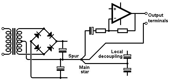
Hmm, then at the risk of showing my ignorance, coudl someone explain why I see this arrangement advised by Doug Self for grounding an amplifier, and not the second version?
EDIT: Looking at it, I suppose it is because the load is so remote that the ground wire leading to the output terminal must be considered an extension of the load impedance.
i use this scheme as my guide....my reasoning is that at the junction of the main filter caps, zero voltage is minimum, not affected by current flow in the other wires....
Merlinb, you are okay in my book, i find your writings very helpful and easy to understand.....
I think for a star grounded system, the diagram above is ok.
I use star (nx-Amp, sx-Amp) and T also (e-Amp). Both can give very good results.
I use star (nx-Amp, sx-Amp) and T also (e-Amp). Both can give very good results.
^should be from the 1980 AUDIO handbook by national semiconductor....
in the manual they say, a ground is a ground, is a ground and a ground...
1980? Wow. The National data sheet for the LM3886 is dated 2003. It says (again paras added):
"Ideally a ground is a ground, but unfortunately, in order for this to be true ground conductors with zero resistance are necessary.
"Since real world ground leads possess finite resistance, currents running through them will cause finite voltage drops to exist. If two ground return lines tie into the same path at different points there will be a voltage drop between them."
The TI data sheet is dated 2004 (it's obviously a reprint of the National data sheet): http://www.ti.com/lit/gpn/lm3886
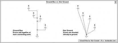
My understanding of which is below:
.
Attachments
Both can give very good results.
No argument here. I'm sure many, many one- and two-IC circuits have been built with no more than a single ground bus, and in the vast majority of cases they do fine.
.
1980? Wow.
grab a copy if you can....i still have mine btw...
"Ideally a ground is a ground, but unfortunately, in order for this to be true ground conductors with zero resistance are necessary.
"Since real world ground leads possess finite resistance, currents running through them will cause finite voltage drops to exist. If two ground return lines tie into the same path at different points there will be a voltage drop between them."
it is imperative to know the currents that will flow, this will tell us what size wire to use....
come to think of it, what could the posters here at diyaudio say that the engineers at national semiconductors haven't thought of before around the early 80's and even before that time?
No argument here. I'm sure many, many one- and two-IC circuits have been built with no more than a single ground bus, and in the vast majority of cases they do fine.
.
and the question that needs to be addressed, how much voltage loss in ground conductors is enough to make the circuit deviate from its original function?
the answer to this question pretty tell us how to proceed imho....
come to think of it, what could the posters here at diyaudio say that the engineers at national semiconductors haven't thought of before around the early 80's and even before that time?
I ask myself the same thing. As far as I know the rules haven't changed since then.
Although...voltages and currents get smaller and smaller. Today Dick Tracey's wrist television is a reality. Surely it's only a matter of time until the thing runs without batteries, on intercellular voltage or something. Maybe not all that much time.
.
that is why i am more interested in what members actually made, never what they say, talk is cheap....we have all we need to know....it is just the doing that is lagging behind, i wish these guys talk less and post more completed amps instead....
after all, these types do not know what another really knows, and using the postings here they can easily be misled.....but completed amps, illustrates what a poster really knows...
after all, these types do not know what another really knows, and using the postings here they can easily be misled.....but completed amps, illustrates what a poster really knows...
The most important thing to consider in the ground connections are
1. the capacitor charging currents - hence the 'spur' shown in D Selfs diagram
2. A star connection off the spur
3. Alternatively, with a 'T' you would connect the speaker return first off the spur, and then the remaining connections - this is how I did it in my e-Amp
1. the capacitor charging currents - hence the 'spur' shown in D Selfs diagram
2. A star connection off the spur
3. Alternatively, with a 'T' you would connect the speaker return first off the spur, and then the remaining connections - this is how I did it in my e-Amp
You need to stop designing the layout as if it were a solid state amp. The ELEKTOR LM3886 design from 1995 is quite bad because the layout resembled a SS amp. Grounding, decoupling and inputs are just not good.
It take another 5 years before Labs 47 design a highend version of a chipamp and they do it by designing a layout, not by using better parts.
If you study their layout you can see that they have abandoned the methods of previous (SS) designers.
They do not whine about "ground is a ground" or "If two ground return lines tie into the same path at different points there will be a voltage drop between them". They design a layout where this does not happen and so can you.
Last edited:
It take another 5 years before 47 Labs design a highend version of a chipamp and they do it by designing a layout, not by using better parts.
If you study their layout you can see that they have abandoned the methods of previous (SS) designers.
Would that be a layout like this? Everything is so tight that you cannot really go wrong with a few individual ground planes?

Last edited:
The chipamp.com and the audiosector amps have obviously been inspired by the original gaincard.
The star ground point is created at the output return (OG), with all the returns connecting to this point through short traces (SG and feedback) or the ground plane (bypass caps and PG+,PG-). It is as if they have read the TI datasheet and implemented it to the extreme. Can it still be improved? I think so, the zobel (Rz and Cz) could be moved closer to the chips output and instead of running the ground plane next to the power planes it would be better to place the power planes over the ground plane.
Then look at the PSU, there is no centre tap transformer used here. It has been designed so that each rail has its own PS and keeps (most of) the charging currents out of the ground plane.
Yes,it would be better to place the power planes over the ground plane.
I described that improvement last week to two Members. One changed his PSU layout to achieve low loop area.
It's all about the ROUTES that the Flow and Return currents have to follow.
post311.
Look at top right and bottom left.
Both have forced the Return current to follow a DIFFERENT Route from the Flow Current.
Would that be a layout like this? Everything is so tight that you cannot really go wrong with a few individual ground planes?

No.
The feedback res length is too long (a la Tomchr sims) but you could just solder the fb res right to the chip pins.
The zobel is too far away.
The right high freq ps cap is too far away.
Not sure about the effect of running the hf ps caps and the med freq (mf) supply caps on the same plane, instead of their own, individual return paths to gnd. (Are there any advanced sims or actual testing?)
The gnd plane is too far away from the chip to add you own hf ps bypass between chip pins and gnd.
🙁
Now, there's one proven PCB design out there and it's totally upped the ante in the field!
😎
I'd love to see some testing and advice on improvement since I bought a big stack of these when they were on sale a couple of years ago :

http://www.diyaudio.com/forums/chip-amps/258372-ive-upped-my-chip-capacitance-up-yours.html
😀
Last edited:

That is also the FetZilla PCB layout.
The rectifiers+smoothing+decoupling are all on the Power Amplifier PCB.
The FetZilla layout causes excess output noise.
They are the noisiest Power Amplifiers I have ever built and I'm convinced it's down to the big loops in the DC power supply routing.
I was never able to cure it.
The amplifiers are effectively redundant.
Last edited:
If you start going P2P style then yes there is some room for improvement but even Tomch places the Rfb on the PCB and does not have a shorter path than the chipamp.com version.
Yes I have Rfb on the PCB running parallel to and close to the long dimension of the chipamp. That gets the loop area fairly low.If you start going P2P style then yes there is some room for improvement but even Tomch places the Rfb on the PCB and does not have a shorter path than the chipamp.com version.
I tried a version with the resistor above the pins and in contact with the package, but could not measure with my DMM, nor scope any changes.
I suspect there is a small improvement to be made and someone like Tom has the gear and the knowledge to find it.
Whether the effort gives anything worth while is debatable.
And one could end up with a partial P2P that can't be "sold" as guaranteed.
If you start going P2P style then yes there is some room for improvement but even Tomch places the Rfb on the PCB...
For clarity, that applies only to the fb res (a la Tomchr)
... and does not have a shorter path than the chipamp.com version.
Look again ...

I'd love to hear solid advice on how to cut 'n' strap to improve the layout. I got a stack of the BrianGT3886 / chipamp.com PCBs a couple years ago, when they were on sale ...
You see, I'm not just a critic, I'm a ... customer! 😉
See the BrianGT3886 / chipamp.com manual:
View attachment chipamp.com BrianGT lm3886-manual.pdf
Last edited:
It is not only loop area that is important but the inductance of the path from chip output to chip input.
- Status
- Not open for further replies.
- Home
- Source & Line
- Analog Line Level
- Comment on Grounding Scheme?