can anybody help me in selecting corner frequency for a class D amplifier and L,C,Q Relations...
i have calculated it for a 2nd Order LPF for 4ohm Load.
L=R/(Q*2*pi*Fc)
Q=R*SQRT(C/L).
C=Q/(R*2*pi*Fc).
where am i Wrong.
i have calculated it for a 2nd Order LPF for 4ohm Load.
L=R/(Q*2*pi*Fc)
Q=R*SQRT(C/L).
C=Q/(R*2*pi*Fc).
where am i Wrong.
I unfortunately have the math skills of a 4th grader, so I use this tool when I need to calculate a filter....
RLC Low-Pass Filter Design Tool
Perhaps it can help you find your answer.
RLC Low-Pass Filter Design Tool
Perhaps it can help you find your answer.
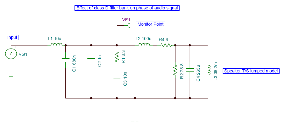
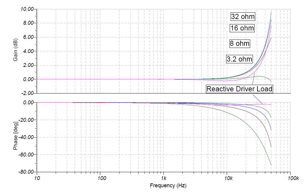
Get a copy of TINA spice program from TI and just simulate it - very easy to use, just draw the circuit, click on components to set value, then run AC frequency response analysis. Can use straight resistive load or a lumped element model of the driver for most accurate results of the filter - tuned to your specific driver.
SPICE-Based Analog Simulation Program - TINA-TI - TI Software Folder
For example, here is the filter for the TPA3116D2:
SPICE-Based Analog Simulation Program - TINA-TI - TI Software Folder
For example, here is the filter for the TPA3116D2:
Get a copy of TINA spice program from TI and just simulate it...
Try out the online calculator link I posted. It gives a lot of useful info on filter performance, though you're limited to simple filters/loads.
Last edited:
Additionally, other interesting output filter design criteria is to move inductor value towards the inductance needed to achieve resonant switching when the amplifier is idle, this saves idle power.
Fsw = idle freq (hz)
Vrails = +/-rail voltage (V)
C = capacitance attached to the switching node (FET + snubbers) (F)
t = dead time (s) (minimum reliably allowed by circuit)
Current needed to charge C from -Vrail to +Vrail in t :
I = 2*Vrail*C/t
Ideal inductor value that would achieve this peak current just before switching node toggles:
L = Vrail*(.25/Fsw)/I
Gate resistors have to be chosen so that gate controlled turn-on dV/dt in switching node is not faster than the dV/dt created by the resonant current in the inductor. This suppresses switching losses for output currents from -I to +I.
I is also the peak output current that the amplifier will do before dead time distortion starts to show up. Higher I makes the low-power lowest-distortion zone wider.
Additionally, other interesting output filter design criteria is to move inductor value towards the inductance needed to achieve resonant switching when the amplifier is idle, this saves idle power.
Fsw = idle freq (hz)
Vrails = +/-rail voltage (V)
C = capacitance attached to the switching node (FET + snubbers) (F)
t = dead time (s) (minimum reliably allowed by circuit)
Current needed to charge C from -Vrail to +Vrail in t :
I = 2*Vrail*C/t
Ideal inductor value that would achieve this peak current just before switching node toggles:
L = Vrail*(.25/Fsw)/I
Gate resistors have to be chosen so that gate controlled turn-on dV/dt in switching node is not faster than the dV/dt created by the resonant current in the inductor. This suppresses switching losses for output currents from -I to +I.
I is also the peak output current that the amplifier will do before dead time distortion starts to show up. Higher I makes the low-power lowest-distortion zone wider.
Eva is that really you ? oh my word. where have you been ? soul searching? welcome back ! 🙂
Last edited:
Maybe , if the inductor is included in the feedback loop. But when not the criteria is a flat frequency response , look at Iraudamp7Additionally, other interesting output filter design criteria is to move inductor value towards the inductance needed to achieve resonant switching when the amplifier is idle, this saves idle power.
Attachments
- Status
- Not open for further replies.
- Home
- Amplifiers
- Class D
- Class D output filter design