Class AB FDA Design
Dear fellow audio enthusiasts,
A second year electro student here. Since a couple of months I’ve been working on this power amp idea.
Design Constraints:
So far I snatched up one 2k5VA 3x25VAC toroidal, two 8k5g and one 6kg heatsinks, which id like to use. Yes, absolutely overkill. Total foorprint will NOT be a limiting factor.
I will keep developing the design before I order anything less general. This community has been of great help since I first posted here. Will purchase 'Power Amplifier Design' by D Self very soon.
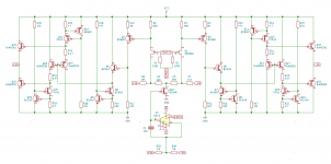
The fully differential design so far uses a 2n3955 monolithic dual jfet at the input and a diamond-like output stage using NJW0281/0302. The VAS is still rather basic. Altogether, it does tick all my boxes. Nevertheless I am looking for a way to give each side its own common mode feedback to account for any asymmetries.
As I'm relatively new to this game, feel free to speak out against any of my reasoning. All of your thoughts and opinions are most welcome. I am here to learn.
Cheers,
Ruben
(this is where it started🙂
.png")
Dear fellow audio enthusiasts,
A second year electro student here. Since a couple of months I’ve been working on this power amp idea.
Design Constraints:
- Bridged inputs and outputs (FDA design)
- CMRR and PSRR => 100dB
- Single supply using 25VAC
- In the ballpark of 100 dubs into 4 ohms (so lots of current)
- Av=>20dB
So far I snatched up one 2k5VA 3x25VAC toroidal, two 8k5g and one 6kg heatsinks, which id like to use. Yes, absolutely overkill. Total foorprint will NOT be a limiting factor.
I will keep developing the design before I order anything less general. This community has been of great help since I first posted here. Will purchase 'Power Amplifier Design' by D Self very soon.
The fully differential design so far uses a 2n3955 monolithic dual jfet at the input and a diamond-like output stage using NJW0281/0302. The VAS is still rather basic. Altogether, it does tick all my boxes. Nevertheless I am looking for a way to give each side its own common mode feedback to account for any asymmetries.
As I'm relatively new to this game, feel free to speak out against any of my reasoning. All of your thoughts and opinions are most welcome. I am here to learn.
Cheers,
Ruben
(this is where it started🙂
Last edited:
Everybody loves those 2SK170 jfets. Digikey says their 2n3955 from Central Semi is a BJT. Why don't you use a silk rope to catch a unicorn?
I build or repair amps with MPSA06/56, or 2n5551/5401, or ST33078 or NE5532 or NJM4560. Parts I can actually buy from authorized distributors.
Of course you can get any transistor you want on aliexpress or ebay. 2019 we bought a replacement 1985 circuit board from a reputable music OEM. It had 29 plastic things with the right part number that looked just like TO92 transistors. They were pieces of plastic with some kind of variable resistance between the pins. The engineer that designed the thing is no longer with the company. Only the techs that build boards are left.
Last edited:
Seems like it ought to work, except you need common-mode feedback. I have no opinion on the JFET input. I don't generally use them, but a lot of people like them.
Most of the distortion will be in Q2 and Q3. I would have chosen to put an emitter-follower buffer before the Q2/Q3 stages rather than after. Q14/Q15 should probably be TIP42 instead of NJW0302, and Q16/Q17 should be TIP41 instead of NJW0281. The current sources Q6, Q7, etc are well done. I would replace R6, R7 with similar current sources.
The main problem I see here is there is no provision for common-mode feedback in this fully differential design. The output voltages will be within mV of each other, but nothing much holds them to VCC/2, other than low gain and bias stability (which is actually pretty low). DC common-mode output voltage, even it is initially VCC/2, will drift like crazy. Differential feedback won't help this, but it will make them track each other.
Be sure in your simulations to look at V x I for each resistor and Vce x Ic for each transistor. Raise power rating and heatsink where necessary. Nothing should be run at more than about 1/4 of its nominal power rating, and transistors at that power level need a small heat sink.
I second what Indianajo said about JFETs. Be sure to specify parts that are obtainable, and are proven in use by other engineers. That's a wheel you do not have to re-invent.
A little more help on the CM feedback:
You are manually tuning T1 to achieve your desired CM output voltage. Try to conceive of a circuit that would sense the average voltage of each output and adjust the current of Q26 to maintain the CM output voltage at VCC/2.
In other words, adjust I(Q26) until ((Va)+(-Va))/2 - Vcc/2 = 0.
There is plenty of literature on common-mode feedback out there. Controlling a current source with the common-mode error is a common method.
If you want to gain an understanding of where distortion is in an amplifier, I really recommend Doug Self's Audio Power Amplifier Design.
Operation in non ideal reality.
Those 2sk170's that I picked up on haha. It doesn't need to be there but it makes for an elegant little current source. Will replace it with a double btj current source like in the rest of the circuit.
The monolithic dual JFET I do really want to use. I have found the 2n3955 on shop.mocross, though expensive still somewhat available.
Thank you all for the great responses. I am looking into your sugestions.
I have checked the power dissipation of each part and everything is nicely inbounds. Only the npn emitter follower and its current source are will dissipate about 100mW, bit on the hot side.
The NJW0XXX's will be snugly mounted to a 6kg heatsink I have here. Q15 is thermally coupled to Q25, Q17 to Q23 ect. As far as I know the NJW's and TIP's are in the right place when we consider dissipation. Any other reasons why there might me swapped in some places?
I will try swapping the npn driver and pnp follower, I see why they might be places the other way round.
Now the question really becomes how can i make sure this unit perform well in non ideal reality mainly considering the thermal runaway of the outputs. Somebody at PS audio already suggested the following:
If possible id like to stay away from a dual supply, so only one transformer secondaire winding and capacitor bank is required per channel. I'm looking into DC servo's and common mode feedback to keep the output DC levels in check.
Much thanks and sheers to you all
This is a great welcome
Ruben
Those 2sk170's that I picked up on haha. It doesn't need to be there but it makes for an elegant little current source. Will replace it with a double btj current source like in the rest of the circuit.
The monolithic dual JFET I do really want to use. I have found the 2n3955 on shop.mocross, though expensive still somewhat available.
Thank you all for the great responses. I am looking into your sugestions.
I have checked the power dissipation of each part and everything is nicely inbounds. Only the npn emitter follower and its current source are will dissipate about 100mW, bit on the hot side.
The NJW0XXX's will be snugly mounted to a 6kg heatsink I have here. Q15 is thermally coupled to Q25, Q17 to Q23 ect. As far as I know the NJW's and TIP's are in the right place when we consider dissipation. Any other reasons why there might me swapped in some places?
I will try swapping the npn driver and pnp follower, I see why they might be places the other way round.
Now the question really becomes how can i make sure this unit perform well in non ideal reality mainly considering the thermal runaway of the outputs. Somebody at PS audio already suggested the following:
- Using dipole supply
- Using NFB,
- Gate resisitors to ground at the inputs
- emmitter restistros at the output stage
- Using DC servo's to keep the common mode voltages in check
If possible id like to stay away from a dual supply, so only one transformer secondaire winding and capacitor bank is required per channel. I'm looking into DC servo's and common mode feedback to keep the output DC levels in check.
Much thanks and sheers to you all
This is a great welcome
Ruben
I don't think that split supplies will gain anything for you, so your decision to stay with single supply is sound.
I did not know that you were thermal tracking the output transistors with Q15 and Q17. The flaw in your plan is that the Vbe tempco can be very different if the collector current is very different. Still, it will probably work, whether you use the expensive transistors or the el cheapo TIP41's and TIP42's. This is difficult to track with simulation because the modeling of tempco's is very bad in many discrete transistor models. Generally speaking, however, any silicon Vbe will track another silicon Vbe. (There are some exceptions.) To test thermal tracking, I've found no substitute for building it on the specified heatsink, and hitting the heat sink with a heat gun.
I still think your choice of transistors is OK, but I would be wary of the much lower Ft of the NJW0302/0281 with much lower collector currents. Probably still higher than TIP41/42. I was just trying to save you a little money.
Dear Russel,
Thanks again for your insights. Just looking at Q15/Q25 atm: Indeed Vbe of Q26 will be larger when more current flows, though as I understand it will drop as temperature increases. Still Vbe of Q25 could become larger than Vbe of Q15, would this be a problem?
I'm guessing I could try to simulate the output transistors (with fixed Ic and Vce temp vs Vbe, Vbe vs Ic)in isolation to see how well they are modeled compared to their datasheets. Its probably gonna be some trial and error in the breadboarding/prototyping phase anyway. I hope with the size heatsinks I got, it won't be too bad.
In previous iterations I was using TIP4X's instead of the NJW's. The NJW's gave me more performance and I like that they could potentially serve in a more powerful circuit and i'm okay with spending a little more here.
PS: the book by Douglas Self is definitely on my list! Bday coming up.
Much thanks and cheers,
Ruben
Attachments
![20210311_130045_HDR[3283].jpg](/community/data/attachments/841/841501-f43ae560dc327b0b929f385b2f43bdfa.jpg?hash=9DrlYNwyew)
Bob Cordell's book is also good, but Doug Self's book is the one to get in order to understand distortion. I've been an amplifier designer for 35 years, and I find both of those books to be great references.
What's funny is that my favorite amplifier topology, the folded cascode, is not even mentioned by Bob Cordell, and Doug Self does not think it is a good topology.
What's funny is that my favorite amplifier topology, the folded cascode, is not even mentioned by Bob Cordell, and Doug Self does not think it is a good topology.
Cordell shows a Folded cascode IPS/VAS in
fig 9.15, 9.16, p209,210
Fig 15.11, p364 second edition also in his vinyltrak phono design
Above is on his web site as his mosfet amp
fig 9.15, 9.16, p209,210
Fig 15.11, p364 second edition also in his vinyltrak phono design
Above is on his web site as his mosfet amp
Last edited:
Hi rsavas,
None of those circuits are folded cascode amplifiers. Those are all cascaded differential pairs with an emitter-follower buffer in between them. He does not call them folded cascodes, either. They all have cascodes, but it is telescopic cascodes, not folded cascodes.
Folded cascodes are noted for not having any current gain from the input pair to the output of the VAS. Voltage gain is close to nil until the output of the VAS, where voltage gain is the product of the input-pair gm and the impedance seen at the VAS output.
The AD797 is one of the classic examples. And almost every audio op amp coming from TI recently. Roender's RMI-FC100 is an example of a well-received amplifier here on diyaudio that is a folded cascode. Doug Self does indeed mention them on page 227 and 228 of his 6th edition. He complains that the input pair has to do all the work. He cannot imagine there is enough gain to do the job, and he complains that there is no Miller capacitance to correct the distortion of the VAS (distortion that folded cascode amplifiers do not have, BTW). To which I reply, "Hold my beer."
Take a look at the amplifier I'm spinning up over on my thread. I'm seeing really great simulated linearity, and I have not even optimized the input pair for THD, yet. I've got 100 dB OLG and a 5MHz Loop-Gain crossover frequency.
RK-Auto200W Amplifer
Summing integrator current source babysitter
Dear fellow audio bliss seekers,
A quick look at common mode feedback got me wondering if this voltage controlled current source i had worked with before could be of any use. Sure enough in multisim it puts the output DC voltage right where we want it.
This solution was mainly driven by wonder and impatience as I have much research left to do on this subject.
I also tried some NFB and emitter resistors. Now the output impedance and top end phase shift are more than halved as simulated in multisim. Remember all these simulations take place in ideal virtual reality.
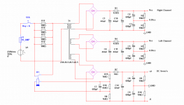
Meanwhile I got a stellar deal on a 2k5VA toroidal. 3x25VAC. I was planning on using one secondary per channel and the third for the 'DC babysitters' and a relay. Please see the schematic of the complete (basic) PSU. These choices are driven by my intuition so I wonder: Is it actually beneficial to give each channel their own secondary side? Even though the secondary sides still interact with each other.
Now here is the catch:
Other options would be:
Once again any feedback is more than welcome. I'd be delighted to here what you think.
Have a great (sounding) weekend and much thanks and cheers,
Ruben
Dear fellow audio bliss seekers,
A quick look at common mode feedback got me wondering if this voltage controlled current source i had worked with before could be of any use. Sure enough in multisim it puts the output DC voltage right where we want it.
This solution was mainly driven by wonder and impatience as I have much research left to do on this subject.
I also tried some NFB and emitter resistors. Now the output impedance and top end phase shift are more than halved as simulated in multisim. Remember all these simulations take place in ideal virtual reality.
Meanwhile I got a stellar deal on a 2k5VA toroidal. 3x25VAC. I was planning on using one secondary per channel and the third for the 'DC babysitters' and a relay. Please see the schematic of the complete (basic) PSU. These choices are driven by my intuition so I wonder: Is it actually beneficial to give each channel their own secondary side? Even though the secondary sides still interact with each other.
Now here is the catch:
- The amplifier needs center point references at the input gate resistors and at the DC servo's positive input. Can these midpoints be defined without using a center tapped transformer (or two sec. sides in series)?
- Additionally the op-amp needs a negative supply with respect to the amplifiers ground. Is there any way to negate this?
Other options would be:
- Using separate toroidals (300VA budget limit) for each channel and tiny (10VA) ones for each servo.
- Using the two 1k25 secondary's in series for a bonkers 60something volts as the amplifier circuit should be easily modifiable for more power. However, now both right and left will share the power supply completely.
Once again any feedback is more than welcome. I'd be delighted to here what you think.
Have a great (sounding) weekend and much thanks and cheers,
Ruben
Attachments
Hi Ruben,
You have the right idea about CM feedback. That does, indeed, work. The integrator cap makes it a differential version of a DC servo, with no worries about CM feedback stability. Probably perfect for your circuit, with a minimum amount of revision or fuss.
Your TL071 should be powered directly from VCC and GND. (VCC must stay below 40V.) The TL071 VCC/2 non-inverting input should also be 1/2 way between the TL071 supplies. There is no need to run the TL072 from a split supply.
If you decide you want a higher VCC, you can replace the TL071 with a PNP diff-pair that drives an NPN current mirror. The output of the current mirror IS the tail current. You can put a C between the summing resistors to limit BW.
That method throws away one of the outputs of the CM feedback diff pair. Another method is to keep a fixed tail current, but have CM feedback control the currents of the 2nd stages. You would replace R12 and R13 with current mirrors controlled by the CM feedback. That is the method used in differential amplifier ICs.
Just FYI, I am not suggesting you replace the TL071. You perfectly have the idea of a "servo". Let's make a slow op amp circuit continuously make the adjustment I've been doing by hand.
That's a big transformer. Whoa. I'm planning to power my 200 Wpc amp with an 800 VA trfr.Meanwhile I got a stellar deal on a 2k5VA toroidal. 3x25VAC.
I was planning on using one secondary per channel and the third for the 'DC babysitters' and a relay.
I would put the DC babysitters for each channel on the same supply as each channel. Then use the third tap to power several nice tubes on the circuit board , to give your amp a warm tube glow. (Don't connect them to your audio signal path.) OK, maybe don't do that.
Still, I would use one secondary for each channel, along with it's supervisor circuits. Basically don't use the 3rd secondary, except maybe to power a Jacob's ladder that runs a spark gap on a shelf over your amplifier. Ok, maybe don't that either. Or you could power a laser light show and listen to Dark Side of the Moon. I cannot think of a good reason to not do this.
More sensibly, for the third secondary, you could make a third channel to power a subwoofer. Hey, that sounds like a practical idea. Until you build that third channel, just tape off the secondary leads, and tuck them away.
Please see the schematic of the complete (basic) PSU. These choices are driven by my intuition so I wonder: Is it actually beneficial to give each channel their own secondary side? Even though the secondary sides still interact with each other.
In short, yes it is still beneficial to give each channel it's own secondary. That way the channels will not share IR drop in the secondaries. Only core loss will be felt by the other channels. It's a close to dual mono as you can get.
Because your amplifier is differential, you are not drawing or returning any current to the center point. You are only using this voltage as the CM reference voltage. Using a resistor divider to create this voltage is just fine.Now here is the catch:
- The amplifier needs center point references at the input gate resistors and at the DC servo's positive input. Can these midpoints be defined without using a center tapped transformer (or two sec. sides in series)?
- Additionally the op-amp needs a negative supply with respect to the amplifiers ground. Is there any way to negate this?
In your PSU schematic, remove C2, C5, and C8. That will greatly increase your PSRR. Also, you are using a huge amount of supply cap for the size of your amplifier. Have you investigated if all that C will even fit in your chassis, along with a 2.5kVA trfr? I bet you could remove C10 and C11 and not notice any change in performance. 22mF would still be enough for each channel. Don't forget, you need to locally bypass VCC to GND on your amplifier PCB, and not just on the PSU board, regardless of the size of the caps in your PSU. At least 3 or 4 mF.
Other options would be:
- Using separate toroidals (300VA budget limit) for each channel and tiny (10VA) ones for each servo.
- Using the two 1k25 secondary's in series for a bonkers 60something volts as the amplifier circuit should be easily modifiable for more power. However, now both right and left will share the power supply completely.
I thought you already bought the 2.5kVA toroid. Just power the servos from the same supply rails as each channel, and skip the tiny transformers. Because your amplifier is differential, I would stay with the 35V VCC. A separate transformer for each channel is cool, if you can afford that. Most DIYers cannot, and just have the channels share the supply.
Putting two of the secondaries in series, with the channels sharing, is what I would do for my power amplifiers, but none of them are differential.
If you already possess the 2.5 kVA, you could put it aside until you build the big brother to the design you've shown.
Your TL071 should be powered directly from VCC and GND. (VCC must stay below 40V.) The TL071 VCC/2 non-inverting input should also be 1/2 way between the TL071 supplies. There is no need to run the TL072 from a split supply.
Indeed there's no need. I realized that I just need a gain device with a higher on voltage. With single supply the op-amp couldn't get the base voltage low enough. Using a mosfet current source eliminates this issue.
If you decide you want a higher VCC, you can replace the TL071 with a PNP diff-pair that drives an NPN current mirror. The output of the current mirror IS the tail current. You can put a C between the summing resistors to limit BW.
That method throws away one of the outputs of the CM feedback diff pair. Another method is to keep a fixed tail current, but have CM feedback control the currents of the 2nd stages. You would replace R12 and R13 with current mirrors controlled by the CM feedback. That is the method used in differential amplifier ICs.
Thanks Russel, I'm liking your ideas. Before there was no real guarantee that Q1 was getting the right drain current. CMFB controlled current sources at the pnp voltages stages works around this.
More sensibly, for the third secondary, you could make a third channel to power a subwoofer. Hey, that sounds like a practical idea. Until you build that third channel, just tape off the secondary leads, and tuck them away.
In your PSU schematic, remove C2, C5, and C8. That will greatly increase your PSRR. Also, you are using a huge amount of supply cap for the size of your amplifier. Have you investigated if all that C will even fit in your chassis, along with a 2.5kVA trfr? I bet you could remove C10 and C11 and not notice any change in performance. 22mF would still be enough for each channel. Don't forget, you need to locally bypass VCC to GND on your amplifier PCB, and not just on the PSU board, regardless of the size of the caps in your PSU. At least 3 or 4 mF.
I thought you already bought the 2.5kVA toroid. Just power the servos from the same supply rails as each channel, and skip the tiny transformers. Because your amplifier is differential, I would stay with the 35V VCC. A separate transformer for each channel is cool, if you can afford that. Most DIYers cannot, and just have the channels share the supply.
Using the third secondary for a sub is a great idea! I definitely don't need it in my room but still its nice to have that option.
Yes I have bought the 2k5 unit second hand much cheaper than new 300VA units. If I don't use it for this project it will find its place.
Is 22mF enough even when drawing 15A occasionally? Is what I was asking myself so I ordered more. 16 pieces 22mF 50V but they've been held at a local sorting facility for weeks🙁
I was planning to give the PSU its own casing and have decided not to let space be a limiting factor. Did not know I needed 3 or 4mF on the amp board. Ill most likely give it 22mF on the amp and 44mF on the PSU.
Thanks again for all your notes.
You're really helping me along.
Cheers,
Ruben
Indeed there's no need. I realized that I just need a gain device with a higher on voltage. With single supply the op-amp couldn't get the base voltage low enough. Using a mosfet current source eliminates this issue.
You need an op amp with rail to rail output. It certainly does not have to be fast. Low noise and offset are what you care about. Take a look at the ADA4522-1. It also goes up to a 55V supply.
https://www.analog.com/en/products/ada4522-1.html#product-overview
Haha that works too.
Your RK audio 200W design goes quite beyond me. Great sophistication. I will my time to read all of it later.
There are things in my own design I don't quite understand. Input to output is non inverting, so is the feedback i'm using actually negative feedback like I assumed?
Cheers,
Ruben
Your RK audio 200W design goes quite beyond me. Great sophistication. I will my time to read all of it later.
There are things in my own design I don't quite understand. Input to output is non inverting, so is the feedback i'm using actually negative feedback like I assumed?
Cheers,
Ruben
- Home
- Amplifiers
- Solid State
- Class AB diff-amp design