Hello Richard,
Thanks for your response, but can I ask what PP cap do you like in this part of the world.
Regards,
Arthur
Thanks for your response, but can I ask what PP cap do you like in this part of the world.
Regards,
Arthur
Waly,
Is there any chance of a photograph of the output stage of your amplifier, please?
Nothing pretty to show. It's P2P wiring (shortest possible connections) triple, on a large slab of aluminum. 8 pairs of MJL, a pair of MJL as drivers and a pair of 2SC5171/2SA1930 as pre-drivers. I'm not pretending this setup would thermally survive 1/3 of 800W/4ohm output forever. I have a couple of small fans wired to blow over the power devices.
 Behave.
This is my CFA amp with BJT EF3 (triple) output with the power of 130 W/8ohm.
Ideally you should have two 2-pole networks, one for each half of the VAS. Resistors should go to the rails. This way the 2-pole compensation also increases PSRR, and supply voltage noise doesn't get into the signal path.
I'm not pretending this setup would thermally survive 1/3 of 800W/4ohm output forever.
What would?
Nothing pretty to show. It's P2P wiring (shortest possible connections) triple, on a large slab of aluminum. 8 pairs of MJL, a pair of MJL as drivers and a pair of 2SC5171/2SA1930 as pre-drivers. I'm not pretending this setup would thermally survive 1/3 of 800W/4ohm output forever. I have a couple of small fans wired to blow over the power devices.
Fair enough. What were your component choices regarding decoupling and emitter resistors?
Ideally you should have two 2-pole networks, one for each half of the VAS. Resistors should go to the rails. This way the 2-pole compensation also increases PSRR, and supply voltage noise doesn't get into the signal path.
That is not actually two pole network(does not show two pole behavior at least) but that resistor(R43) decrease ULGF, from 6.4 MHz with no resistor to the 2.4 MHZ with 220 ohm there. Why do you think that connecting resistors to the rails will increase PSRR, I would think opposite, but I have to simulate to be sure.
With only one OIC cap I could get better compensation symmetry.
Fair enough. What were your component choices regarding decoupling and emitter resistors?
0.33 ohm emitter, 2.2 ohm base. Tried .22 ohm, got current hogging, is not going to work without devices matching, something I'm not able or willing to do. Due to the large number of output pairs (eight), bias is not critical around the Oliver point, gm doubling is not an issue. Biased at about 70mA/pair. Drivers bias 60mA, pre-drivers bias 10mA.
1800uF/100V from each MJL collector to the common ground bar.
Last edited:
Let's kindly stick to CFA amplifiers on this thread - I don't think it's too much to ask. This will require that posters are open with their topology and circuits.
If it's not CFA, kindly open another thread where your design can be discussed freely.
If it's not CFA, kindly open another thread where your design can be discussed freely.
A 0.1 C/W finned heat sink.
Any better heatsink recommendations?
I've been using KL-271 heatsinks from a group buy several years ago.
Attachments
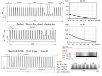
Those look good- class A material 😀
When I'm back in EU or the USA (or wherever I'll end up next) I'll be sure to order a few meters.
The other guys that do interesting stufj are Fischer - but they are expensive, and buying from them is a pain.
When I'm back in EU or the USA (or wherever I'll end up next) I'll be sure to order a few meters.
The other guys that do interesting stufj are Fischer - but they are expensive, and buying from them is a pain.
And you have verifiable scientific evidence of this? 🙂
Hi Scott,
preamble --
We all know that current in a round conductor has the HF near the surface nad we know that a flat thin conductor (like a pcb trace) will have the high freqs running along the two outside edges. And, we know that if a pcb trace uses right angles, the trace Z is highest at the corners (thus use 45 degree angles at corners). ETC.
I made a selective delay line for power buss using this information - Imagine 2 long, flat, wide traces side by side. Across and along the trace gap are 10, 1000mfd ultra low esr and esl caps. If you use a very sensitive phase detector such as in my HP4194A and run the two test leads to one end of the two strips and the other end of the two strips back to the Z analyzer (a 4-wire measuring instrument), you will get a Z plot of that combination thru the strips with almost pure C across them (90 degrees).
If the high freqs are truely along the edge we can lengthen the HF path only by cutting slits in the edge as shown below and we should see the affect of the HF delay as a change in total Z plotted:
I used this technique to cancel out the extra phase (Z) change of the capacitor at HF to extend the low cap Z to higher freq than the caps alone could do by themselves.
But there is a trick to it regarding the pcb copper thickness which has an affect... do you know what increasing the copper thickness would do to the delay strip line?
THx-RNMarsh
Attachments
Last edited:
Some have expressed that circuits with fewer parts do not perform as well as more complex circuits. But, John Curl has started to open up his designs which are very few parts but very high performance.... go to his place in the Lounge and look at #48761 thru 48770. Its a balanced bridged amplifier topology.
There are still some questions to be answered re CFA. But later, maybe his circuits will inspire us to deviate now from the strict CFA topology to find what is needed to make a simplifed version but without a distortion penalty and any audible characteristics in tact. Especially, see his distortion cancellation from the symmetry/topology.
THx-RNMarsh
Last edited:
Clever trick!If the high freqs are truely along the edge we can lengthen the HF path only by cutting slits in the edge as shown below and we should see the affect of the HF delay as a change in total Z plotted:
I used this technique to cancel out the extra phase (Z) change of the capacitor at HF to extend the low cap Z to higher freq than the caps alone could do by themselves.
 🙂
🙂Richard, people are not claiming fewer parts means lower performance. If you mesure distortion, then low compnent count designs are generally higher - but we all know theres no correlation between distortion and aural pleasure. That said, JC's designs are not noted for being single digit, so it does seem to fit OS's observation.
NP is also a minimalist.
I just don't have the balls to build a 10 pair class A mosfet output stage driven by a 6 transistor front end. Maybe someone from the Pass forum will get on my case and convince me . . . 😉
NP is also a minimalist.
I just don't have the balls to build a 10 pair class A mosfet output stage driven by a 6 transistor front end. Maybe someone from the Pass forum will get on my case and convince me . . . 😉
Hi Scott,
preamble --
We all know that current in a round conductor has the HF near the surface nad we know that a flat thin conductor (like a pcb trace) will have the high freqs running along the two outside edges. And, we know that if a pcb trace uses right angles, the trace Z is highest at the corners (thus use 45 degree angles at corners). ETC.
I made a selective delay line for power buss using this information - Imagine 2 long, flat, wide traces side by side. Across and along the trace gap are 10, 1000mfd ultra low esr and esl caps. If you use a very sensitive phase detector such as in my HP4194A and run the two test leads to one end of the two strips and the other end of the two strips back to the Z analyzer (a 4-wire measuring instrument), you will get a Z plot of that combination thru the strips with almost pure C across them (90 degrees).
If the high freqs are truely along the edge we can lengthen the HF path only by cutting slits in the edge as shown below and we should see the affect of the HF delay as a change in total Z plotted:
I used this technique to cancel out the extra phase (Z) change of the capacitor at HF to extend the low cap Z to higher freq than the caps alone could do by themselves.
But there is a trick to it regarding the pcb copper thickness which has an affect... do you know what increasing the copper thickness would do to the delay strip line?
THx-RNMarsh
RF and SMPS guys get this . . . . one small slit (I'd cal it a notch) in a motherboard DC-DC converter drain connection can cause significant issues.
Typical rise times attainable BTW are 2-3 ns at 30 A
Richard, people are not claiming fewer parts means lower performance. If you mesure distortion, then low compnent count designs are generally higher - but we all know theres no correlation between distortion and aural pleasure. That said, JC's designs are not noted for being single digit, so it does seem to fit OS's observation.
NP is also a minimalist.
I agree with you. Well, I am trying to lead you some where with this. It isnt clear yet how to say it. Its connected to all the other things i bring up so have to go back over all that ---- cancellation thru topology, symetrical topology, clever cancellation configurations. It doesnt have to be super simple.... just that taking a topology - and refining the heck out of it.... wasnt what I was thinking. Actually, what I am thinking does not now exist. But, I think JC's conceptual thinking comes closest to mine and so brought it up at this opportune time.
Just thinking out loud and the feedback... I thrive on it. The good. The bad. And, the ugly.
THx for this and the other great forums.
Richard
Last edited:
connecting the dots -
I'm going to answer this myself --- the edge effect in very thin pcb copper is greater/stronger than thick pcb copper. Either a high Z cap or a thick pcb copper can minimize the ability to see much change or affect on the caps Z in this edge effect test. The design depends on the distance and width and the caps and the thickness to work. The caps were specially made for me in Taiwan for this edge effect test. The copper thickness is the same as used in many consumer products (such as the new Marantz MM7025 CFA power amp). Very, very thin... too thin IMO.
THx-RNMarsh
I made a selective delay line for power buss
But there is a trick to it regarding the pcb copper thickness which has an affect... do you know what increasing the copper thickness would do to the delay strip line?
THx-RNMarsh
I'm going to answer this myself --- the edge effect in very thin pcb copper is greater/stronger than thick pcb copper. Either a high Z cap or a thick pcb copper can minimize the ability to see much change or affect on the caps Z in this edge effect test. The design depends on the distance and width and the caps and the thickness to work. The caps were specially made for me in Taiwan for this edge effect test. The copper thickness is the same as used in many consumer products (such as the new Marantz MM7025 CFA power amp). Very, very thin... too thin IMO.
THx-RNMarsh
Last edited:
0.33 ohm emitter, 2.2 ohm base. Tried .22 ohm, got current hogging, is not going to work without devices matching, something I'm not able or willing to do. Due to the large number of output pairs (eight), bias is not critical around the Oliver point, gm doubling is not an issue. Biased at about 70mA/pair. Drivers bias 60mA, pre-drivers bias 10mA.
1800uF/100V from each MJL collector to the common ground bar.
Hello Waly ,
Online vendors I know sell matched output devices for power output stages for audio power amplifiers.
Regards
Arthur
- Home
- Amplifiers
- Solid State
- CFA Topology Audio Amplifiers