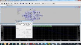
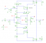
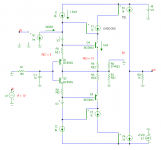
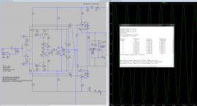
1.2mhz to 1.5 mhz is the VFA upper limit !
These alien CFA's play by different rules.
4.7mhz is where I can get 640V/us(10p). Slight overshoot at this plot.
Absolutely overkill , 47p gives 2.5mhz 250v/us .. this will be the
design target.
PS - Every thing I have ever simulated with KSA992/Ksc1845 - Ksa1381/ksc3503
has almost perfectly been realized in the real build. oscilloscope readings/DMM readings ...
I WOULD NOT waste my time designing a PCB for a "dud" ...
OS
I am sorry about be misleading. (Ok not entirely). 😱
The bandwidth of 1.2MHz is when it is designed without output inductor.
🙂😀 With an inductor - 7MHz. 47degrees phase margin.
Attachments
Last edited:
Here's how I got the NX to run with 0-5pf.
The idea came from hawksford's papers.
(below). real simple.
2 more caps .... .68uF works as well .
My feedback question is circled in the attachment , as well.
OS
Short the 10 ohm and measure thd. and/or remove diodes and measure thd.
-RNM
Those devices is not a problem, or any small signal devices for that matter. I can easily get to 10MHz. with those devices.
The real problem lays in the output stage. It is just not fast enough. With an fT of 30 - 40MHz it starts to get a serious problem.
I am trying to find a solution for this at the moment.
I will let you now. Have to dig up some old sims.🙂
How do OPS mosfets compare in speed?
-RNM
They are better, but my experience is that they oscillate very easy with to small gate resistor.
Exicon should have something like 100 - 200R. -> -3dB around 700KHz - 1.5MHz for the mosfet itself.
I really need to retest them.
Exicon should have something like 100 - 200R. -> -3dB around 700KHz - 1.5MHz for the mosfet itself.
I really need to retest them.
Bob Cordell
 [/URL][/IMG]
http://radikal.ru/fp/37291870ee864b6b837d62ecf5bcb246] [/URL]
Best regards
Petr
- I prefer solid state amplifiers with JFET input stages. I have not seen any CFAs here with JFET inputs. Are JFET inputs not compatible with CFAs?

http://radikal.ru/fp/37291870ee864b6b837d62ecf5bcb246]
 [/URL]
Best regards
Petr
Again, i don't agree.This is a CFA. And, Bonsi's is a CFA. Its really pretty easy to know a CFA by its topology --> We have shown it early on here.....
Again... This is the topology for a CFA:
View attachment 389987
Other topologies are something else and don't behave exactly as this topology does.
For me, the definition of a VFA is the one given by Analog device and shown in the macromodel (from many datasheet and application notes) in attachment2 of my post: #3108.
The same, exactly, is given by TI. (http://www.ti.com/lit/ds/symlink/opa2695.pdf)
Are-we allowed to change this ?
Your attachment 389987 is a variation of it and the 'dual complementary common collector voltage follower', out of the loop just an enhancement. As well as 'diamond' or any kind of emitter follower. As well as the second emitter follower to drive OPS.
Richard, are-you crossed against-me, to not answered directly my questions ?
Last edited:
Here's how I got the NX to run with 0-5pf.
The idea came from hawksford's papers.
(below). real simple.
2 more caps .... .68uF works as well .
My feedback question is circled in the attachment , as well.
OS
Sorry I did not see your question.
The 10 ohm resistor is just to isolate the clean ground from the dirty ground.
To do gain tests and sims, you would normally have a ground on both sides of the 10 ohm resistor.
Last edited:
If you apply the two tests, it will cater for BJTs, FETs, single ended and balanced input stages of the diamond or any other input structure and give you the right answer almost every time.
When I looked into 'what is a CFA?' I got lots of math explanations, a lot of stuff that left me no wiser. That's how I ended up with the two tests.
I don't think to simply say as long as the feedback signal is applied to the low impedance inverting port without any interposing active stage it's a CFA. An H bridge input structure breaks that definition, but it's still a CFA. Likewise, if you have a classic CFA diamond input structure but the feedback resistor value is made very high, the gain bandwidth independence of CFA is no longer met, and what you actually have is a very sub optimal VFA. In this case, test no. 1 would indicate, correctly, a VFA because CLG -3db BW would be dependent on gain, despite the fact that the TIS peak input current would be set by Rf.
IMV what defines a CFA is much more to do with how it performs/behaves and less about the way the parts are connected.
🙂
Last edited:
I'm NOT fighting with your tests. They are a way to analyses a black box, and presume of the topology used, depending of the results...That's how I ended up with the two tests.
Not a topology description.
I tried to propose a definition, as precise, short and accurate as possible, to describe what is perfectly described by the macro models i showed.
Got no comments, i wonder why: Are-we talking of something we are not sure to agree with, if i refer to Bob Cordel's questions ?
[edit] I'm not inventing anything. Just refer to the literature. Feel free to modify and improve my definition/proposal.
"An H bridge input structure breaks that definition, but it's still a CFA." please, explain, with schematic ?
"IMV what defines a CFA is much more to do with how it performs/behaves and less about the way the parts are connected" It is a consequence, not the toplogy (OMHO).
Last edited:
Esperado, like I said in my post, you need to focus on circuit behavior as the key indicator of what the topology is - the circuit structure on its own will not guarantee you draw the correct conclusion.
I don't think to simply say as long as the feedback signal is applied to the low impedance inverting port without any interposing active stage it's a CFA. An H bridge input structure breaks that definition, but it's still a CFA.
🙂
H bridge input op-amps have the VFA property of falling closed-loop BW with increased closed-loop gain. They do have slew on demand but so do the old slew-enhanced input op-amps.
Scott, we need you to bring your CFA definition, or arbitration.H bridge input op-amps have the VFA property of falling closed-loop BW with increased closed-loop gain. They do have slew on demand but so do the old slew-enhanced input op-amps.
But does this not also happen when you run a standard CFA with high CLG? They also degenerate into VFA.
it is an other thing: How to design in order to get the benefit of this topology.Esperado, like I said in my post, you need to focus on circuit behavior as the key indicator of what the topology is - the circuit structure on its own will not guarantee you draw the correct conclusion.
Instead of quibbling about the definition of CFA and VFA amps, let's see how we can improve a CFA input stage. We know already that for lowest distortion RE = 0.5/gm = 0.5 VT / Ic or 13mV / Ic at room temperature (and ignoring bulk resistances for a moment). A weak point of a so called 'CFA' input stage is the not so good PSRR and the susceptibility of noise from the current sources (CCS) which are needed to bias the input stage. The PSRR can be improved by using cascodes, while the impact of CCS noise can be reduced by using a diamond configuration and proper choices of the emitter resistors. As far as I can see, this is only possible if the collectors of the first transistor pair are connected either to the emitters of the second transistor pair (fig.1) or to the feedback node (fig.2). If the collectors are tied the to supply rails, it is not possible to cancel out the CCS noise.
Of course one could calculate analytically the proper values of the emitter resistors, but as I am lazy, I used my simulator to figure it out, though it's an iterative process.
In the example below, Ic of the output trannies (Q3 & Q4) were set to 1mA. So for lowest distortion RE2 should be: 0.5 * VT / Ic = 13 Ohms. Check this as shown in fig.1.
By means of a VCCS G1 an AC current -representing the noise- has been injected (see fig.2). Adjust RE1 (and keep Ic =1mA by also adjusting Ib of the CCSes I1 and I2) for the lowest output signal. With RE1 = 5 Ohms the output signal was about 50dB lower compared to a circuit where the collectors of Q1 and Q2 were tied to the supply rails. If the collectors are connected as shown in fig.1, RE1 should be 7.5 Ohms.
In this simulation perfectly matched trannies were used. So in real life the CCS noise reduction will be less impressive. Also notice that the optimal resistor values should not only be adjusted for the emitter bulk resistance but also depend on VT, being a function of temperature.
Cheers, E.
models:
.MODEL BC550G NPN (IS=1.8E-14 BF=1k NF=1 VAF=1k ISE=5E-14
+ NE=1.46 BR=35.5 NR=1 VAR=1k IKR=.03 ISC=1.72E-13 NC=1.27
+ CJE=13P CJC=4P VJC=.54 MJC=.33 TF=.64N TR=50N)
.MODEL BC560G PNP (IS=1.8E-14 BF=1k NF=1 VAF=1k ISE=5E-14
+ NE=1.46 BR=35.5 NR=1 VAR=1k IKR=.03 ISC=1.72E-13 NC=1.27
+ CJE=13P CJC=4P VJC=.54 MJC=.33 TF=.64N TR=50N)
Attachments
Good engineering, Edmond (as habit ;-)
Any impact on the input stage by the add of the cascode (slew rate, pole etc.)?
Any impact on the input stage by the add of the cascode (slew rate, pole etc.)?
JFET CFA
There's no problem in adding J-fets to the Front-end, but you need a cascode as they otherwise would see too much voltage. Here it's fixed at 12 V, but it could also be made as a Hawksford. I chose the simple and included the cascode as a part of the 12 V supply for servo op-amp and current source for the input-pair.
Distortion is even a factor 10 lower
Attachments
Here are three CFA "dumb questions/observations" that have probably been brought up here before, but not seen by me.
1. The Williamson tube amplifier and most others had the negative feedback connected to the cathode of the input stage. Does this make it a CFA?
2. The early solid state amplifiers had the negative feedback connected to the emitter of the fist-stage transistor. Did this make them CFAs?
3. I prefer solid state amplifiers with JFET input stages. I have not seen any CFAs here with JFET inputs. Are JFET inputs not compatible with CFAs?
I ask these questions in the spirit of the broader view of what is a CFA in this thread, as opposed to the more narrow technical definition that has sometimes been cited here.
I gave earlier, several times, my definition of what is commonly called a "CFA" (and proved mathematically that it explains all known properties). It's though, most likely, to abstract to be of any DIY use.
A "CFA" is a "VFA" having the open loop gain (and loop gain) controlled/modulated by the feedback network.
By this definition, 1, 2 can be indeed "CFA"s and for 3, there is no limitation in using whatever input devices to get a "CFA", jfets are just fine.
"Can be", because for large closed loop gains, a "CFA" approaches asymptotically the pure "VFA" properties.
How do OPS mosfets compare in speed?
-RNM
Vertical MOSFETs are fundamentally VERY fast. Their equivalent ft can be on the order of 100-400MHz. I say equivalent when defining ft to be somewhat like we define it for BJTs. In the case of a MOSFET, OMEGAt ~ gm/input capacitance. MOSFETs are more inclined to oscillate than BJTs without careful design and layout, largely due to their high speed. Merely putting large resistance in series with the gate often ruins much of their ft advantage. See a discussion on this topic in MOSFET power amplifier JAES article, available on my web site. As a simple explanation, lower values of gate stopper can be used if gate Zobel networks are used.
Cheers,
Bob
Bob Cordell
By New Year's every whim:
- I prefer solid state amplifiers with JFET input stages. I have not seen any CFAs here with JFET inputs. Are JFET inputs not compatible with CFAs?
[/URL][/IMG]
http://radikal.ru/fp/37291870ee864b6b837d62ecf5bcb246][/URL]
Best regards
Petr
Thanks, Petr, this makes sense, especially if one has good complementary JFETs. This seems to fit the broader topological definition of a CFA that has been described here.
Cheers,
Bob
- Home
- Amplifiers
- Solid State
- CFA Topology Audio Amplifiers


