Indeed.Is the resistance in the emitter of the input device playing a double role :
- as a degenerative resistance giving local feedback
- as the "foot" resistance of the negative feedback network which divides the output voltage.
But don't remember to disconnect serial feedback resistance from output and connect-it to the ground if you want to explore the open loop behavior, as they are paralleled as the emitter resistance.
The cap to ground is used by Lazy Cat's VSSA to add some AC gain to the input stage in order to optimize distortion. Not a requisite of CFAs.But it's not pure as the current injected is the current function of a voltage AC shunt. (caps to Gnd).
Last edited:
Stirring the pot a bit
Several people like the current on demand feature of a CFA and in the past I liked it too. But as a matter of fact this feature makes the input stage too good. Yes, you read it correctly, too good. The trouble with CFA's is that under overload conditions, it outputs too much current which causes 'sticking'. In order to avoid this, one needs extra circuitry, preferable an 'active clamp' (something that acts on the negative feedback input). That's the only way (AFAICS) to keep this 'current on demand' within reasonable limits. But such active clamp in itself is problematic because of the high loop gain. It's not so easy to get it stable.
Therefore, I'm back to VFA. Since the output current of the IPS is 'self-limiting', one doesn't need a complicated active clamp. So how about high slew rate and low distortion without currents on demand? Just design a circuit that doesn't need high currents from the IPS at all. How? Simply, use Miller input inclusive compensation (MIC). Bob Cordell, for example, has shown how to do that.
It is said that a VFA produces more noise, because of the relative large emitter degenerating resistors. Well, just omit them (or lower its value) and adjust the gain of the TIS accordingly. I have shown how to do that here. (btw, the slew rate of that circuit is over 500V/us. Large enough?)
Cheers, E.
I know you can make CFA's DC coupled as well (FB)
But as you say and also what I see in my simulations, the AC feedback has distortion benefits. and it also makes the design less prone to a drifting DC offset at the output.
But as you say and also what I see in my simulations, the AC feedback has distortion benefits. and it also makes the design less prone to a drifting DC offset at the output.
Several people like the current on demand feature of a CFA and in the past I liked it too. But as a matter of fact this feature makes the input stage too good. Yes, you read it correctly, too good. The trouble with CFA's is that under overload conditions, it outputs too much current which causes 'sticking'. In order to avoid this, one needs extra circuitry, preferable an 'active clamp' (something that acts on the negative feedback input). That's the only way (AFAICS) to keep this 'current on demand' within reasonable limits. But such active clamp in itself is problematic because of the high loop gain. It's not so easy to get it stable.
Cheers, E.
Hi Edmond,
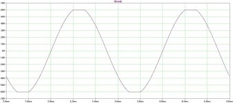
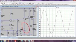
Does simulation wil that "sticking"?
This is simulated clipping of my 200 W CFA with lateral output and no "sticking" at all.
BR Damir
Attachments
Yeah, that is somewhat true, also the things that went through the cable is usually current..🙄Ultimately, this also applies a to VFA.😀
Remember, the IPS is a transconduction stage (voltage in, current out out ).
Cheers, E.
The name CFA seems not in the right place, it should be Forward Current Amplifier or FeedForward then Current is Back Amplifier or something like that.😀
Hi Edmond,
Does simulation wil that "sticking"?
This is simulated clipping of my 200 W CFA with lateral output and no "sticking" at all.
BR Damir
Hi Damir,
That looks OK. But I have a few questions:
How well does the circuit behave with even larger input voltages and higher frequencies (e.g. 20kHz)?
Are you sure there are no transistors that saturate. Beware of the fact that they might suffer from sticking, while a simulation doesn't show it.
Where can I find the schematic (as there are so many updates)?
Cheers, E.
Last edited:
Originally Posted by forr
Is the resistance in the emitter of the input device playing a double role :
- as a degenerative resistance giving local feedback
- as the "foot" resistance of the negative feedback network which divides the output voltage
?
Indeed.
But don't remember to disconnect serial feedback resistance from output and connect-it to the ground if you want to explore the open loop behavior, as they are paralleled as the emitter resistance.
Ok.
Now, if the CFA emitter resistance is modified, it modifies the transconductance of the input stage in two ways :
- the degenerative action ;
like for a differential pair of a VFA input.
- the quiescent current through the device ;
unlike a VFA input where the quiescent currents are settled "externally" to the devices by a constant current source.
Does it make the control of two circuits behaving differently, one relying on currents subtraction (CFA), the other relying on transconductance (VFA) ?
Hi all,
With the risk of stating the obvious or stating something that has been stated before in this thread (which I haven't been following since the beginning), I would like to make a few comments:
Slewing
Slewing is caused by clipping of the stages in front of the stage that sets the dominant pole or poles. Hence, there are two ways to get a good slew rate:
1. Make sure there are no stages in front of the one that sets the dominant pole, as explained by Edward
2. Ensure that the stages in front of the one that sets the dominant pole don't clip. For example, you can use a large bias current combined with local series feedback (emitter degeneration). The emitter degeneration need not be active at low frequencies, so you can put a big inductor across the resistors if you like.
Another approach is to use some sort of class-AB biasing for these stages. One way to do that is with complementary common-base stages and current mirrors, the input stage topology used in most of the controversial feedback amplifiers. Other methods can be found in:
Giovanni Stochino, "Non-slewing audio power amplifier", Electronics World March 1996, pages 256...259
M. G. Degrauwe and W. M. C. Sansen, "Novel adaptive biasing amplifier", Electronics Letters 3 February 1983, pages 92 and 93
Terri S. Fiez, Howard C. Yang, John J. Yang, Choung Yu and David J. Allstot, "A family of high-swing CMOS operational amplifiers", IEEE Journal of Solid-State Circuits, December 1989, pages 1683...1687.
Amplifiers that remain inaccurate when the gain of one stage is made infinite
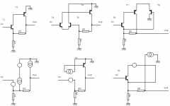
See the attached figure. The upper three schematics are the signal schematics of three amplifiers. Everything related to biasing is left out.
As someone already mentioned (in different terms), the voltage gain of the upper left circuit does not approach the feedback resistance ratio plus one when the gain of one stage approaches infinity. When the gain (I mean voltage, transadmittance, transimpedance and current gain) of the first stage goes to infinity, you still have an error term from the second transistor's base current. When the gain of only the second stage approaches infinity, you still get an error term due to the Early effect of the first transistor. You only get a transfer set by the resistance ratio plus one when both stages have infinite voltage, transadmittance, transimpedance and current gain.
One way to solve this issue, is to use a differential pair as the first stage, see the upper middle figure. The base current of the second stage now no longer flows into the feedback network, but the circuit has become off topic as this is voltage feedback in all senses of the word.
Another approach is the upper right circuit. Assuming matched transistors in the second stage, the base current error of the output transistor T7 is corrected by the equal but opposite base current error of T8. There is ideally no signal voltage across the input transistor T6 and, hence, no problem with T6's Early effect.
This circuit looks like it is on topic, with the feedback network connected to an emitter, but any current flowing in is compensated by the base current coming out of T8. Hence, I'm afraid this one is as off topic as the middle circuit.
The bottom three figures illustrate what I've just written for those familiar with two-ports and nullors. They show how you can get to a closed-loop voltage gain of the resistance ratio plus one by replacing the minimum number of stages with nullors (two-ports with infinite voltage, current, transimpedance and transadmittance gain).
A single circle is a nullator, a network element that conducts zero current and has zero voltage across it, a double circle is a norator, a circuit element that can conduct any current and have any voltage across it. Together a nullator and a norator form a nullor, an infinite gain two-port that can only be used in feedback configurations. A nullor is basically the same as an ideal op-amp, but with an extra output terminal that conducts an equal but opposite output current.
For all circuits except the first, it suffices to let one stage get nullor properties. For the first circuit, both stages need to get nullor properties. Note that a nullator with a norator in series is equivalent to an open branch.
Best regards,
Marcel van de Gevel
With the risk of stating the obvious or stating something that has been stated before in this thread (which I haven't been following since the beginning), I would like to make a few comments:
Slewing
Slewing is caused by clipping of the stages in front of the stage that sets the dominant pole or poles. Hence, there are two ways to get a good slew rate:
1. Make sure there are no stages in front of the one that sets the dominant pole, as explained by Edward
2. Ensure that the stages in front of the one that sets the dominant pole don't clip. For example, you can use a large bias current combined with local series feedback (emitter degeneration). The emitter degeneration need not be active at low frequencies, so you can put a big inductor across the resistors if you like.
Another approach is to use some sort of class-AB biasing for these stages. One way to do that is with complementary common-base stages and current mirrors, the input stage topology used in most of the controversial feedback amplifiers. Other methods can be found in:
Giovanni Stochino, "Non-slewing audio power amplifier", Electronics World March 1996, pages 256...259
M. G. Degrauwe and W. M. C. Sansen, "Novel adaptive biasing amplifier", Electronics Letters 3 February 1983, pages 92 and 93
Terri S. Fiez, Howard C. Yang, John J. Yang, Choung Yu and David J. Allstot, "A family of high-swing CMOS operational amplifiers", IEEE Journal of Solid-State Circuits, December 1989, pages 1683...1687.
Amplifiers that remain inaccurate when the gain of one stage is made infinite
See the attached figure. The upper three schematics are the signal schematics of three amplifiers. Everything related to biasing is left out.
As someone already mentioned (in different terms), the voltage gain of the upper left circuit does not approach the feedback resistance ratio plus one when the gain of one stage approaches infinity. When the gain (I mean voltage, transadmittance, transimpedance and current gain) of the first stage goes to infinity, you still have an error term from the second transistor's base current. When the gain of only the second stage approaches infinity, you still get an error term due to the Early effect of the first transistor. You only get a transfer set by the resistance ratio plus one when both stages have infinite voltage, transadmittance, transimpedance and current gain.
One way to solve this issue, is to use a differential pair as the first stage, see the upper middle figure. The base current of the second stage now no longer flows into the feedback network, but the circuit has become off topic as this is voltage feedback in all senses of the word.
Another approach is the upper right circuit. Assuming matched transistors in the second stage, the base current error of the output transistor T7 is corrected by the equal but opposite base current error of T8. There is ideally no signal voltage across the input transistor T6 and, hence, no problem with T6's Early effect.
This circuit looks like it is on topic, with the feedback network connected to an emitter, but any current flowing in is compensated by the base current coming out of T8. Hence, I'm afraid this one is as off topic as the middle circuit.
The bottom three figures illustrate what I've just written for those familiar with two-ports and nullors. They show how you can get to a closed-loop voltage gain of the resistance ratio plus one by replacing the minimum number of stages with nullors (two-ports with infinite voltage, current, transimpedance and transadmittance gain).
A single circle is a nullator, a network element that conducts zero current and has zero voltage across it, a double circle is a norator, a circuit element that can conduct any current and have any voltage across it. Together a nullator and a norator form a nullor, an infinite gain two-port that can only be used in feedback configurations. A nullor is basically the same as an ideal op-amp, but with an extra output terminal that conducts an equal but opposite output current.
For all circuits except the first, it suffices to let one stage get nullor properties. For the first circuit, both stages need to get nullor properties. Note that a nullator with a norator in series is equivalent to an open branch.
Best regards,
Marcel van de Gevel
Attachments
Sticking
>I have no sticking issues on CFA either. Clipping in fact is very soft.
Hi Andrew,
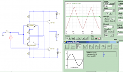
Apparently it depends on circuit details. One of Damir's earlier versions does have clipping issues, see pic, Glen K. and I had also issues.
Cheers, E.
>I have no sticking issues on CFA either. Clipping in fact is very soft.
Hi Andrew,
Apparently it depends on circuit details. One of Damir's earlier versions does have clipping issues, see pic, Glen K. and I had also issues.
Cheers, E.
Attachments
Last edited:
Why ? Nothing impeach-you, and it is even recommanded, to use a CCS, collector side, to set the DC current of a VFA's input stage.- the quiescent current through the device ;
unlike a VFA input where the quiescent currents are settled "externally" to the devices by a constant current source.
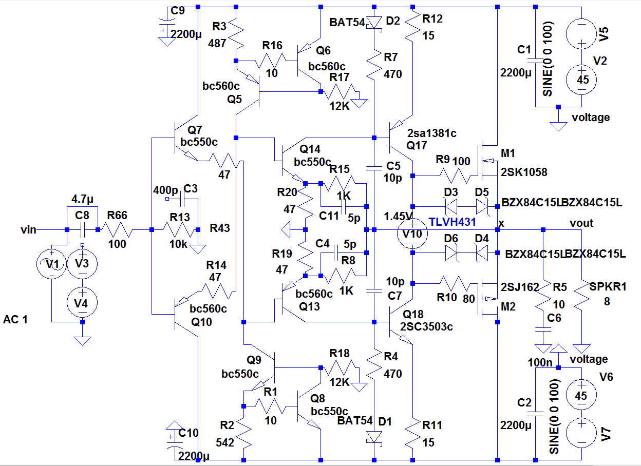
Like this, witch use no caps in the feedback paths:
http://www.diyaudio.com/forums/atta...846-vssa-lateral-mosfet-amplifier-dc-vssa.gif
The real input stage are Q13 & Q14.
Q7 & Q10 are used for 3 purposes:
1, cancel the base emitter voltage offset;
2, reduce source impedance,
3, add isolation between the feedback loop and the input signal and parasitic capacitances of the wiring..
Q7 & Q10 are not part of the closed loop, so, don't add a pole..
I am not sure to understand what you mean by 'the control of the circuits'.Does it make the control of two circuits behaving differently, one relying on currents subtraction (CFA), the other relying on transconductance (VFA) ?
Same remark on my side. Of course, you will take care to set a low pass filter at the input to ensure slew rate margin under all circumstances. This will avoid TIM as well. The high bandwidth of VFAs will help to get higher margin and high enough FC to get a flat phase response.I have no sticking issues on CFA either. Clipping in fact is very soft.
Hi Damir,
That looks OK. But I have a few questions:
How well does the circuit behave with even larger input voltages and higher frequencies (e.g. 20kHz)?
Are you sure there are no transistors that saturate. Beware of the fact that they might suffer from sticking, while a simulation doesn't show it.
Where can I find the schematic (as there are so many updates)?
Cheers, E.
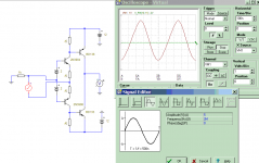
Hi Edmond,
Here is schematic and zip file with .asc.
BR Damir
Attachments

Sorry for the typo, you have corrected: "current of a CFA's input stage"Why ? Nothing impeach-you, and it is even recommanded, to use a CCS, collector side, to set the DC current of a VFA's input stage.
Last edited:
>I have no sticking issues on CFA either. Clipping in fact is very soft.
Hi Andrew,
Apparently it depends on circuit details. One of Damir's earlier versions does have clipping issues, see pic, Glen K. and I had also issues.
Cheers, E.
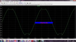
Hi Edmond,
This is one interested case. It uses enhanced VAS/TIS and the collector protection resistor in the enhancer transistor should be of higher value. With 220 ohm that was standard used in VFA) there is "sticking", but increased to 4.7 k the sticking disappeared.
BR Damir
Attachments
Why ? Nothing impeach-you, and it is even recommanded, to use a CCS, collector side, to set the DC current of a VFA's input stage.
Like this, witch use no caps in the feedback paths:
http://www.diyaudio.com/forums/atta...846-vssa-lateral-mosfet-amplifier-dc-vssa.gif
The real input stage are Q13 & Q14.
Q7 & Q10 are used for 3 purposes:
1, cancel the base emitter voltage offset;
2, reduce source impedance,
3, add isolation between the feedback loop and the input signal and parasitic capacitances of the wiring..
Q7 & Q10 are not part of the closed loop, so, don't add a pole..
Your Q7 and Q10 act a buffer. I am pretty sure they are a good thing because they allow to have a relatively high impedance of signal source, like the cursor of a pot, without penalty.
Q7 and Q7 set the input bias to Q13 and Q14 but do not impose, as does the CCS , a current to the devices where the feedback is applied.
However, you are right, even without buffering devices, a current can be imposed to Q13 and to Q14 by a CCS in their emitter, but part of the current going through the emitter resistor. I think such a design has been proposed here in a previous post.
Feedback is a control process. A lot of discussion about CFA is about the way its feedback intimately works.I am not sure to understand what you mean by 'the control of the circuits'.
In VFA, the control of the circuit is done by the voltage difference between the input bases and the transductance of the differential pair.
Many people think CFA work in a similar same manner, controlled by the voltage between base and emitter of the input transistors and the transconductance of the stage.
Some other people do not seem to agree.
in the "CFA" topology under discussion the feedback does sample the output V, differences it from the + input V, causes a current porportional to the input stage Vdiff*gm to drive the next stage
the "CFA" input gm however is also affected by the feedback R network Z adding to the input rx
and the next stage may differ too
the input gm controls the GBW - "CFA" are "decompenesated" - not unity stabe with a wire to the ouptut - the user tunes the degree of decompensation by selecting the feedback ratio divider's equivalent series R
today most monolithic VFA are unity gain compensated with no way to change the GBW - a few are made with compensation pins, a few more can be bought in fixed decompensation for say 5x, 10x min stable gain
common audio examples are the monolithic power chip amps like LM3886 with min stable gain >10x
like "CFA" discrete VFA designs also have the freedom to compensate for the design V gain, just by changing different part's values than the feedback R ||Z
Last edited:
sticking & dipping
Hi Damir,
But then Q1 gets saturated. As I don't trust simulations with regards to saturation effects, I hope that also in real life this 4.7k resistor will solve the sticking issue. Anyhow, a CFA IPS can deliver far more current than a VFA IPS, so more attention should be paid to overload conditions.
Cheers, E.
Hi Edmond,
This is one interested case. It uses enhanced VAS/TIS and the collector protection resistor in the enhancer transistor should be of higher value. With 220 ohm that was standard used in VFA) there is "sticking", but increased to 4.7 k the sticking disappeared.
BR Damir
Hi Damir,
But then Q1 gets saturated. As I don't trust simulations with regards to saturation effects, I hope that also in real life this 4.7k resistor will solve the sticking issue. Anyhow, a CFA IPS can deliver far more current than a VFA IPS, so more attention should be paid to overload conditions.
Cheers, E.
- Home
- Amplifiers
- Solid State
- CFA Topology Audio Amplifiers