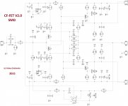
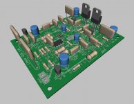
I have refined the initial CF-FET symmetric front-end design, using experience, gained with the first one, as well as understanding some of its drawbacks. Now it's even simpler (6 transistors), however, promising lower distortion, higher slew rate and even better ability to drive the Lateral FET OPS directly, allowing high VAS current - at the moment it's tuned to 18mA, although 30mA is not a problem with those rugged TO-220 MOSFETs.
Tuned TMC compensation reduces distortion at the higher end of the audio bandwidth.
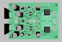
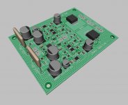
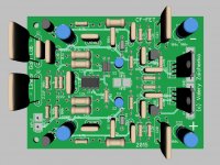
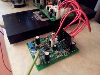
I'm going to try SMD with this one for the first time - after prototyping a through-hole version, so that I don't have to change any parts on SMD board.
I'm sure, soldering will be fun 🙂 Everything is easy to buy except SMD version of the MOSFETs - 3 weeks lead time.
Comments are welcome.
Cheers,
Valery
Tuned TMC compensation reduces distortion at the higher end of the audio bandwidth.
I'm going to try SMD with this one for the first time - after prototyping a through-hole version, so that I don't have to change any parts on SMD board.
I'm sure, soldering will be fun 🙂 Everything is easy to buy except SMD version of the MOSFETs - 3 weeks lead time.
Comments are welcome.
Cheers,
Valery
Attachments
Hopefully , you will garner interest in SMD construction.
Many will resist , but they will be assimilated. 😀
If by anything , the lack of through-hole sourcing.
The SS relays and control board were my "first taste".
Not really too hard , even with conventional tools. 🙂
Edit - this is the "Singleton" IPS ? Nice !
Sorry , that is the CFA ...
OS
Many will resist , but they will be assimilated. 😀
If by anything , the lack of through-hole sourcing.
The SS relays and control board were my "first taste".
Not really too hard , even with conventional tools. 🙂
Edit - this is the "Singleton" IPS ? Nice !
Sorry , that is the CFA ...
OS
Last edited:
Looks good Valery.
I think more of us will be forced to go SMD, and likely sooner rather than later. And really, why not? Some of the newest and best components are now SMD, with virtually no new TH parts are being developed save for power devices.
Admittedly, I have been a little 'gun-shy' to try it but maybe it's time. Keep up the good work! Your pace is up there with the forums best, almost breathtaking. I'm 'glacial' by comparison.
Jason, thanks for the feedback 🙂
I was also sort of "shy" and also think the time has come. Compact yet high-quality parts, ability to place them on both sides if necessary, ease of local "heatsinking" with the foil areas - a lot of flexibility.
Let's see how the first "pilot" goes 😉
I was also sort of "shy" and also think the time has come. Compact yet high-quality parts, ability to place them on both sides if necessary, ease of local "heatsinking" with the foil areas - a lot of flexibility.
Let's see how the first "pilot" goes 😉
Hopefully , you will garner interest in SMD construction.
Many will resist , but they will be assimilated. 😀
If by anything , the lack of through-hole sourcing.
The SS relays and control board were my "first taste".
Not really too hard , even with conventional tools. 🙂
Edit - this is the "Singleton" IPS ? Nice !
Sorry , that is the CFA ...
OS
Well, it's a simple symmetric CFA, but it simulates incredibly well. Large electrolytics may scare somebody 🙂p), but eliminating them, we normally come to "evil diamond"... so, I want to see how this topology performs in practice.
SMD is the way to go 😉
Super!!!I have refined the initial CF-FET symmetric front-end design, using experience, gained with the first one, as well as understanding some of its drawbacks. Now it's even simpler (6 transistors), however, promising lower distortion, higher slew rate and even better ability to drive the Lateral FET OPS directly, allowing high VAS current - at the moment it's tuned to 18mA, although 30mA is not a problem with those rugged TO-220 MOSFETs.
Tuned TMC compensation reduces distortion at the higher end of the audio bandwidth.
I'm going to try SMD with this one for the first time - after prototyping a through-hole version, so that I don't have to change any parts on SMD board.
I'm sure, soldering will be fun 🙂 Everything is easy to buy except SMD version of the MOSFETs - 3 weeks lead time.
Comments are welcome.
Cheers,
Valery
Go ahead Vallery
It is time for SMD.

2 disadvantages
1 difficult finding parts🙁
2 no diy dual layer boards🙁
Last edited:
So far, my local shop has got everything in stock, except SMD version of MOSFETS... not that bad.
Hopefully, as SMD becomes more popular, distributors will bring-in more of them.
And this is something we can help with (making it even more popular 😉)
Hopefully, as SMD becomes more popular, distributors will bring-in more of them.
And this is something we can help with (making it even more popular 😉)
Are the isolated patches of ground fill gridded up? I've come across a number of different philosophies when it comes to ground fill (and its removal) but none of them have a place for isolated bits of copper.
Everything is easy to get here for this.😀 For those new to SMD, buy a syringe of solder paste and cook it in a toaster oven. Touch it up with an iron later. Much easier and components actually align themselves as they bake. Data sheets always have baking instructions.
Initial testing
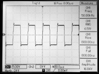
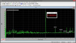
OK, tested "as is" with Lateral FET OPS (the one from TubSuMo project), 8R load.
Not bad for the beginning. Excellent distortion profile, rather low IM. Certain overshoot at square wave response - requires some tuning. Also, there is a very slight local oscillation at the input stage (first two transistors cascade) - hopefully, not too difficult to tame.
Cheers,
Valery
Attachments
OK, tested "as is" with Lateral FET OPS ...
Hi Valery
What output level were the measurements?
Have you compared this with simulation to validate the (non LTSpice) models?
Best wishes
David
Last edited:
Excellent project. Glad to see more n more SMD designs. One comment about the electrolytic caps. I have long been SMD-ed with pretty much everything I build but I keep using good ol' thru-da-ho e-caps. The primary reason is their height can get them caught and knocked off during handling a PCB assembly causing permanent damage to PCB by ripping the pads out. I also found less variety choice and more expensive on the SMD camp for e-caps, despite they are neither of higher performance nor smaller in size than their thu-ho counterparts.
Hi Valery
What output level were the measurements?
Have you compared this with simulation to validate the (non LTSpice) models?
Best wishes
David
Hi David,
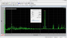
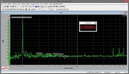
My sound-card input attenuator is set in a way that optimum level at the output is 4-4.5V RMS (2-2.5 W @ 8 ohm load). These particular measurements are done at 4.2V RMS.
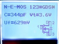
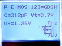
Simulation is rather close to the live measurements. Interesting, that I have checked two bunches of MOSFETs (N- and P- channel respectively) - Vt values are very close, tolerance is within +/-0.1V (see attached example). Good enough for just taking them randomly.
Previous version - with symmetric jFET input - had lower loop gain, showing around 0.012% of the 2-nd harmonic @ 1KHz. This one is higher loop gain and much lower distortion - close to the measurement system resolution.
This MOSFET VAS shows good linearity, when driven with low impedance (EF) - mitigating its high, slightly non-linear, input capacitance.
Cheers,
Valery
Attachments
Excellent project. Glad to see more n more SMD designs. One comment about the electrolytic caps. I have long been SMD-ed with pretty much everything I build but I keep using good ol' thru-da-ho e-caps. The primary reason is their height can get them caught and knocked off during handling a PCB assembly causing permanent damage to PCB by ripping the pads out. I also found less variety choice and more expensive on the SMD camp for e-caps, despite they are neither of higher performance nor smaller in size than their thu-ho counterparts.
Nattawa, thank you for the electrolytic caps advise - I was actually thinking about this. No real benefit from using SMD ones, same as with some good polymer multi-layer decoupling caps - those just don't exist as SMD parts. So, for everything, except HF compensation ceramics, "ol' thru-da-ho" ones make a lot of sense to me

I will update the SMD design as soon as I finalize tuning-up all the compensation.
Cheers,
Valery
noo... I hate MLCC, especially the heavily micro-phonics X5R & X7R!
Ah, of course not X5R/X7R 🙂 For signal path decoupling - only metal film. Polistirene, polypropilene, etc. Sorry for confusion.
OK, tested "as is" with Lateral FET OPS (the one from TubSuMo project), 8R load.
Not bad for the beginning. Excellent distortion profile, rather low IM. Certain overshoot at square wave response - requires some tuning. Also, there is a very slight local oscillation at the input stage (first two transistors cascade) - hopefully, not too difficult to tame.
Cheers,
Valery
Hi Valery
could you measure the distortion with real speaker and compare it with the distortion taken on resistive load to show if there are present some residues of back-emf on real speakers?
Just for curiosity...
Hi Pawel,
Yes, at this level of distortion - pretty interesting to what extent it's going to change the picture. I will try to do it, hopefully in the end of the week - Sunday. Till that time - travelling, attending Mobile World Congress in Barcelona 🙂
Cheers,
Valery
Yes, at this level of distortion - pretty interesting to what extent it's going to change the picture. I will try to do it, hopefully in the end of the week - Sunday. Till that time - travelling, attending Mobile World Congress in Barcelona 🙂
Cheers,
Valery
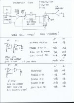
Hi Valery
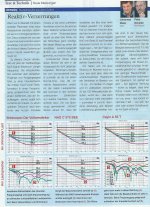
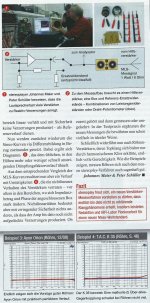
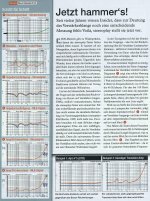
Hier is some help for real world AMP testing.More scans later.
Hier is some help for real world AMP testing.More scans later.
Attachments
-
 Stereoplay 1.10-11.jpg660.9 KB · Views: 201
 -
 Stereoplay 1.10-10.jpg722.3 KB · Views: 194
 -
 Stereoplay 7.09-10.jpg758.3 KB · Views: 235
 -
 Stereoplay 6.09-1.jpg1,015.1 KB · Views: 279
 -
 Stereoplay 1.10-2.jpg830 KB · Views: 297
 -
 Stereoplay 1.10-1.jpg1 MB · Views: 381
 -
 EMK-Testing _ AMP-Topologies.jpg406.1 KB · Views: 370
 -
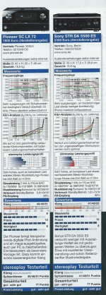 Stereoplay 1.10-12.jpg651.6 KB · Views: 211
- Status
- Not open for further replies.
- Home
- Amplifiers
- Solid State
- CF-FET V2.0 front-end - going high-tech (SMD)