Hi Semola,
I'm sorry you felt I was aggressive, but I was merely matching what I perceived was the tone of your post. The views I felt were those of someone who reads the popular press in audiophile land and were unwarranted. It seemed like you made your mind up without any understanding of the circuit that was presented.
Had you posed your comments as questions, you would have received an explanation instead of what I posted. Keep in mind that whatever you post will be read by people who are experts in the field, and also others like yourself who have other expertise but not in audio design. We don't want to further myths, but rather have an opportunity to learn.
One reason these "Diamond buffer" circuits are popular is that they are blazingly fast while also having low distortion. The signal is distorted by the first transistor stage as is normal, while the output stage in the diamond distorts it in a complementary way, which tends to undo the distortion caused by the input stage. The actual diamond formation consists of only four transistors in the audio path.
There are diamond buffers produced as an IC in one package, and have been for years. The BUF634 is one good example of this. To gain some understanding, why not look up this part's data sheet? You will see the actual diamond buffer along with some support circuitry. But by reading the specs you will gain some insight into the capabilities of this design.
-Chris
Hi nauta,
I don’t understand your question. There is no Vbe multiplier in a diamond buffer, so nowhere to put a cap. Output stage quiescent current is explicitely set by a source and sink connected to the diamond.
I don’t understand your question. There is no Vbe multiplier in a diamond buffer, so nowhere to put a cap. Output stage quiescent current is explicitely set by a source and sink connected to the diamond.
Hi Suzy J
Post-268: Q20 + R34 + R37 are clearly a bias-set circuit for the output diamond. The latter has no emitter resistors on the input pair and needs something to balance against the two Vbe drops per side of the output stage.
Every bias regulator I see has at least 100nF across it, and usually 10uF or so.
Yeah. It’s also got no power supply filtering caps. That’s because it’s a simulation, not a finalised design. For the purposes of the simulation it makes zero difference. By all means add a cap there in sim if that’s what blows your hair back.
BTW, you do know that making comments like this about someone’s simulation don’t make you look clever, but actually the opposite. Of course if you did the work to show that it actually had an effect (any effect) that’d be different.
BTW, you do know that making comments like this about someone’s simulation don’t make you look clever, but actually the opposite. Of course if you did the work to show that it actually had an effect (any effect) that’d be different.
Hi Suzy
I have a lot of respect for you - more than you cared to display when I ask a simple question. I didn't look at that specific schematic as purely a simulation; rather, like the others you've posted on this thread that were intended to be built. In that context, I thought maybe you had a reason not to include the usual Vbe cap?
My question comes from the perspective of someone who deems you to have superior knowledge, not as a criticism of your work.
Last edited:
I hope you are given plenty of time to do some research on your own, so that you can rephrase your questions in a form perhaps like
"When I performed measurement X, I got numerical value Y, which seems to be sufficiently different from your numbers suzyj, to make me ask: what have I done wrong?"
"When I performed measurement X, I got numerical value Y, which seems to be sufficiently different from your numbers suzyj, to make me ask: what have I done wrong?"
Building an amp with LM3886 is not a challenge. The DIY thing is the challenge most of the time. It's seldom just to solve a task as easy you can.The amp is ridiculous complex for such low output power capability.
And it will not work as shown - it is oscillating even in simulation.
Why not use a LM3886 or similar. It is cheaper and more adequate for
building your first amp.
If you pursue the simplest approach
The simplest approach would be to use something like a TPA3101D2 class D amp or whatever. More efficient and robust than an old fashioned analogue amp. Boring, Boring, ... No creativity or risk involved.
You can bet sooner or later someone will try and scale this suzyj amp up to a higher power level or think of some other interesting modification.
Per-Anders hit it on the head. It's about 95% the intellectual stimulation of designing something with performance I haven't got a chance of hearing, then making a beautiful layout and building it for me.
The end product is just a thing that pushes some speaker cones in and out.
The end product is just a thing that pushes some speaker cones in and out.
I'm on a bit of a design binge right now - I blame the new version of KiCad, which is such a pleasure to design with.
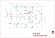
A few posts up after mucking around with the cascaded diamond topology I concluded that the best way to get a low-cost, medium-power amp that doesn't burn heaps of power was to go back to a more normal emitter followed output stage. So this is the polished version. I reckon it'll make 20W with a D44H11/D45H11 output driver stage, with basic BD139/140 drivers, and +/-24V supplies. The nice thing about only having two hot parts is that heatsinking is ever so easy, unlike the amps with many output drivers.
The reason this is interesting to me is that the MV supplies for my bigger 100W class G amp are +/-28V, so that's near enough to what this wants. I could use this for tweets and midrange, and put the woofer on the 100W amp. Or even use the 200W amp with two paralleled woofers, and the 100W amp for mid. Anyway, the tweeters don't need a lot of power, but they do need a lot of speed, and this topology has buckets of speed.
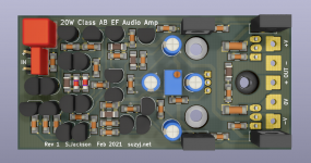
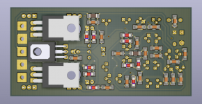
PCB is 38 x 77mm. It idles at around 1.5-1.7W, depending on output bias. The BOM is ~$25, so it's not an expensive amp, and there's nothing exotic and hard to get. Indeed 90% of the parts I've already god.
A few posts up after mucking around with the cascaded diamond topology I concluded that the best way to get a low-cost, medium-power amp that doesn't burn heaps of power was to go back to a more normal emitter followed output stage. So this is the polished version. I reckon it'll make 20W with a D44H11/D45H11 output driver stage, with basic BD139/140 drivers, and +/-24V supplies. The nice thing about only having two hot parts is that heatsinking is ever so easy, unlike the amps with many output drivers.
The reason this is interesting to me is that the MV supplies for my bigger 100W class G amp are +/-28V, so that's near enough to what this wants. I could use this for tweets and midrange, and put the woofer on the 100W amp. Or even use the 200W amp with two paralleled woofers, and the 100W amp for mid. Anyway, the tweeters don't need a lot of power, but they do need a lot of speed, and this topology has buckets of speed.
PCB is 38 x 77mm. It idles at around 1.5-1.7W, depending on output bias. The BOM is ~$25, so it's not an expensive amp, and there's nothing exotic and hard to get. Indeed 90% of the parts I've already god.
Attachments
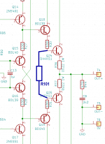
No particular reason, really, I just drew a pair of transistors. It really points to my inexperience with this style of output stage more than anything.
I'm guessing it's there for stabilising the gain of the driver stage with devoce and temperature variation? I'm guessing it's a good thing to have.
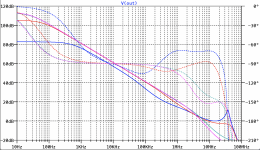
Here's an open loop ac plot of adding and varying this resistor in sim, showing it has some profound RF stability implications, though this is more likely due to starving the output transistors of current and hence changing the bias point rather than any magic of it's own.
In the plot blue is 100≈, red 1K, green 10K, and magenta 10Meg.
I'm guessing it's there for stabilising the gain of the driver stage with devoce and temperature variation? I'm guessing it's a good thing to have.
Here's an open loop ac plot of adding and varying this resistor in sim, showing it has some profound RF stability implications, though this is more likely due to starving the output transistors of current and hence changing the bias point rather than any magic of it's own.
In the plot blue is 100≈, red 1K, green 10K, and magenta 10Meg.
Attachments
I might create an initial starting point, by estimating the maximum base current that can possibly flow in the output transistors, and then choosing R101's resistance value so its DC bias current will be two or three times greater.
If (8R * Irms * Irms) = 20 watts then Irms is 1.6 amps and Ipeak is 2.25 amps.
If Beta = 80 then Ibase = 28mA. So I might choose R101 to have 85mA of DC bias current. At least as a starting point for further calculations.
And I'd actually connect R101 from emitter to emitter, not from base-stopper to base-stopper. Whoopsie, drawing error.
_
Last edited:
That'll push standby consumption from 1.7W to 3.7W, which will then require heatsinking of the drivers.
I can see your rationale - it means the servo only has to correct for one pair of Vbe rather than two. However the same effect is gained with much less current, as long as you ensure that the drivers and main output pair come our of class-A at different points, so the servo system still has to deal with one pair of Vbe at a time.
I've rejigged things a little, and rather than simply tying the emitters of the drivers together with a resistor I've used a pair of resistors to the output node. Some fiddling with compensation and output stage bias and I reckon it's a good one.
Simulation attached.
Attachments
The added resistor, which usually is rather connected directly between the emitters of driving transistors, is there to suck out the base charge of the following transistors, some times even a small capacitor is added in parallel to help speed up turn-off .
That'll push standby consumption from 1.7W to 3.7W, which will then require heatsinking of the drivers.
I can see your rationale - it means the servo only has to correct for one pair of Vbe rather than two. However the same effect is gained with much less current, as long as you ensure that the drivers and main output pair come our of class-A at different points, so the servo system still has to deal with one pair of Vbe at a time.
I've rejigged things a little, and rather than simply tying the emitters of the drivers together with a resistor I've used a pair of resistors to the output node. Some fiddling with compensation and output stage bias and I reckon it's a good one.
Simulation attached.
Hello i try to run the simulation but i saw square wave at output. Could you please help me to find out the mistake i did.
Attachments
- Home
- Amplifiers
- Solid State
- Cascading diamond buffers - a cheap low THD 10W amp with TIP41C