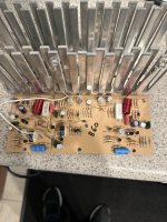
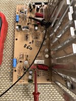
Hello, good day everyone on this forum. i would like to know if there is anyone here that could explain the basic operating principles of this amplifier. 1 channel is down and ive replaced all the diodes and semiconductors but still have 69vdc on q7 transistor.......i have already removed all the mosfets from this channel and still get 69vdc at the base of q7 ? any help would be appreciated thanks Frank........the board number is 1806 ...this is a soundcraftsmen pm860
Attachments
Did you replace all the parts with the exact same part numbers? If not, then you may be in a lot more trouble than if you had asked for help at the beginning.
Basically the way this thing is/was suppose to work is that Q1 and Q2 make a differential pair. In the absence of an input signal then both transistor collector currents should be the same. Q1 and Q2 are fed from a current source which is Q3. The voltage drop across R6 combined with knowing the resistance of R6 should tell you how much current is shared by Q1 and Q2. In the absence of an input signal then normally both Q1 and Q2 currents would be the same, so the voltage drops across R7 and R8 would be the same, and the sum of the currents thought then should be the same as the current through Q3. That is of course if that part of the circuit were operating normally.
However, with the MOSFETs removed the circuit is now no longer normal at all, since the feedback loop is open.
Did you already know all that, or where are you starting from in trying to understand this amplifier?
Last edited:
It appears that there should indeed be +69VDC on the base of Q7 (which is PNP type),
as you find, since the Q7 emitter is connected to the +70VDC rail.
This is a simple common emitter amplifier stage, just referred to the positive rail.
What was the original problem with this amplifier, since that is not the problem.
as you find, since the Q7 emitter is connected to the +70VDC rail.
This is a simple common emitter amplifier stage, just referred to the positive rail.
What was the original problem with this amplifier, since that is not the problem.
Last edited:
hello Markw4.no, i did not know all that. I have just been measuring parts and hoping to get lucky. I tried to use most the same parts. for Q7 AND Q8 I used mpsa92 instead of mpsa93 the mm4003 and 2n3440 i used the same replacements. would it be good idea to reinstall the mosfets? and continue ..what would you recommend i check after that
hello rayma. this amplifier has about 60 volts dc on the speaker output of 1 channel . When i connected it to the speaker i got a spark. lucky i did not ruin my speaker
It may be better to restore the circuit to its original form before proceeding. However I would first ask as rayma just did, what was the symptom you were trying to fix that started all this parts changing? Was it simply that you noticed a high voltage at the output? If so, did the amp ever work right?

this amplifier has about 60 volts dc on the speaker output of 1 channel . When i connected it to the speaker i got a spark. lucky i did not ruin my speaker
Yes, but that is not due to Q7. Never connect a defective amplifier to a speaker.
That is what test equipment is for.
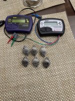
First thing to do before removing any parts should be to test all PN junctions in circuit with your DVM.
But if the parts have already been removed, go ahead and test them out of circuit with the diode function of DVM.
Don't reinstall the outputs without testing them, since one may be shorted.
Last edited:
Q7/Q8 is just a clipping indicator. And since the emitter of Q7 is connected to the positive rail by means of a 22 ohm resistor the base cant be far of that voltage.
Those are types of MOSFET.
But a digital voltmeter GOOD/BAD diode test of each PN junction would be simpler, and not require interpretation.
But a digital voltmeter GOOD/BAD diode test of each PN junction would be simpler, and not require interpretation.
Double checking the transistors is a good place to start before replacing them. What would follow at some point would be to put it back together, power it up, and take a number of voltage readings at various points around the circuit. Maybe do some calculations to see if the readings make sense of if they indicate a problem in that area of the circuit. At some point an oscilloscope and signal generator may be helpful. If you don't know how to do all that stuff, then you should probably work with the people here to take you through it step by step. Maybe at the end of it you will have learned some good things from this experience that you can apply to some future troubleshooting problem.
Q1 and Q2 is long tailed pair.
Q3 is LTP current source
Q4 is VAS current source
Q5 is bias spreader
Q6 is VAS
Q7 and Q8 is clipping indicator
Q9 and Q12 output drivers
Q10, Q11, Q12, Q13, Q14, Q15 are outputs
The amp should be able to play on two pair of outputs
2SJ50 / 2SK135 are out of stock for many years.
Q3 is LTP current source
Q4 is VAS current source
Q5 is bias spreader
Q6 is VAS
Q7 and Q8 is clipping indicator
Q9 and Q12 output drivers
Q10, Q11, Q12, Q13, Q14, Q15 are outputs
The amp should be able to play on two pair of outputs
2SJ50 / 2SK135 are out of stock for many years.
Ok, i will be reinstalling the mosfets and reassembling. I will check back with you all soon. This things given me a headache. I would like to learn how to trouble shoot without having to rip everything apart. i dont really care for a shotgun approach but its all ive had up to this point.
Base and emitter of Q9 voltage reading would be good. Reading voltage across the 180 Ohm gate resistors is also useful. Any drop is bad.
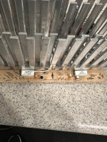
The peak semiconductor tester is okay I use one. Do the output Mosfets have insulators?
The peak semiconductor tester is okay I use one. Do the output Mosfets have insulators?
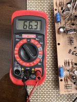
Hi Wayne. Q9 b=67.4vdc and e=66.8...............180ohm resistors 3 have 66.6vdc and 3 have 66.2...All mosfets have to3 silicon pads
Last edited:
Hi
What’s the issue with the amp?
What are you troubleshooting?
Was the amp working before?
BR
Eric
What’s the issue with the amp?
What are you troubleshooting?
Was the amp working before?
BR
Eric
See https://www.diyaudio.com/community/threads/soundcraftsmen-pm860-red-led-light-stuck-on.384855/What are you troubleshooting?
- Home
- Amplifiers
- Solid State
- can anyone offer help understanding the flow of this circuit