Hi Patrick, good to hear from you! Still owe you some answers...... not forgotten!
Yes, shunt regulators can be painful, and I use cap multipliers a lot. The "Paradise" phono really was a joint work of multiple people, with Joachim Gerhard doing the concept, Michael Borresen did the circuit, Frans der Wal did the regulators, and I just did the PCB layout and group buy. And Calvin (Christoph) later contributed the Calvin buffer, which is a big improvement over the original output buffer. The shunt reg proved to be difficult in multiple builds, when people changed transistors mostly, and it could take some time to find out.....
In this case however, I think that it could be a case of the Base-Collector junction being forward biased (since the neg supply doesnt come up), and the circuit just seems to like that new bias point a bit too much..... But we will see.
@ stefanoo, usually the calvin buffer is well-behaved and I had it up and running easily in several other projects as well, without this problem. I may still have my prototype somewhere, and will try if I can make it do the same thing when I limit the startup current...... Not sure when I will get to that.....
As promised, I have breadboarded the circuit tonight to have more easy access to implement changes.
I think have found the reason as to why the buffer has this behavior and, IF the following is correct, then my guess would be that all bufffers have this behavior, but, I would be extremely interested, when you get a chance, to kindly doublecheck and see if you have different findings.
After some more thinking, I came to the conclusion that the AC bootstrap capacitor C46, which couples the bottom part of the buffer to the top side, is rather large and charges at start up, which introduces a delay that can bring the buffer in a temporary wrong biasing state like the one I am experiencing.
Obviously, for proper operation AC operation and stability, the capacitor is needed, but I started wondering, if the value coulf be reduced and of, by reducing its value, also the inrush current decreases.
Since the way I understand this buffer, the small AC signal coupled from the bottom to the top is effective at higher frequency, the value could potentially be reduced without decreasing the frequency response, but perhaps the stability point might change,
Therefore. I proceeded to reduce the capacitor from 0.22uF (value used all applications I have seen around) down to 10nF.
While frequency response seems unaffected, the inrush current has resolved. As I had feared a bit, the stability has changed and I can see some minor ringing on the edge of the square wave depending on the grounding on my probe, which means the circuit is a bit more prone to oscillations, but overall, it seems stable.
My question is directed to you and to the folks who knows more inside-out this buffer: have I introduced any problem I am not aware of by lowering the cap value?
Last edited:
The reason for the coupling between the two halves, with C46, is to further improve the distortion behaviour. In fact, the midpoint of the resistors R198 and R202 is chosen to maximize symmetry between the halves, and cancel out the differences. So you could simply remove it and would end up with the same function, at slightly higher distortion. Some versions of the Calvin buffer even had a trimpot there, but - unless you have a rather perfect input sine wave and a really good distortion measurement - you will be hard-pressed to improve by adjusting (I tried). Best to simulate the optimum point and match the components, I think.
Assuming J13 does not forward-bias on the gate, there will be no other current to charge C46 except through the 1M resistor. This gives a corner frequency of ~0.7Hz. No huge need for distortion reduction at that frequency 😀 At 10nF , this would be 16Hz, should be no issue at all. Hope this helps!
Assuming J13 does not forward-bias on the gate, there will be no other current to charge C46 except through the 1M resistor. This gives a corner frequency of ~0.7Hz. No huge need for distortion reduction at that frequency 😀 At 10nF , this would be 16Hz, should be no issue at all. Hope this helps!

Thank you very, very much, this makes total sense and confirms what I see on the bench as well.
Yes, I could make precision distortion measurements, but I don't think it's worth the while. I would go for the standard 100/75 as per the schematic and lower the cap maybe to something like 10-22nF to have quick turn on.
I am assuming you are using the 0.22uF bootstrap cap, for all your implementations therefore, when of course you indeed will have a chance to run this test, please observe the following two things:
1) Inrush current on the negative rail
2) Once the rails have reached the rail voltage, observe the bias current at the output going from a higher value, down to the target after few seconds.
HensenThe reason for the coupling between the two halves, with C46, is to further improve the distortion behaviour. In fact, the midpoint of the resistors R198 and R202 is chosen to maximize symmetry between the halves, and cancel out the differences. So you could simply remove it and would end up with the same function, at slightly higher distortion. Some versions of the Calvin buffer even had a trimpot there, but - unless you have a rather perfect input sine wave and a really good distortion measurement - you will be hard-pressed to improve by adjusting (I tried). Best to simulate the optimum point and match the components, I think.
Assuming J13 does not forward-bias on the gate, there will be no other current to charge C46 except through the 1M resistor. This gives a corner frequency of ~0.7Hz. No huge need for distortion reduction at that frequency 😀 At 10nF , this would be 16Hz, should be no issue at all. Hope this helps!
Just to update on this topic. Despite having resolved the startup condition by lowering the bootstrap capacitor, I am analyzing the response of the buffer and I find something quite concerning to me.The reason for the coupling between the two halves, with C46, is to further improve the distortion behaviour. In fact, the midpoint of the resistors R198 and R202 is chosen to maximize symmetry between the halves, and cancel out the differences. So you could simply remove it and would end up with the same function, at slightly higher distortion. Some versions of the Calvin buffer even had a trimpot there, but - unless you have a rather perfect input sine wave and a really good distortion measurement - you will be hard-pressed to improve by adjusting (I tried). Best to simulate the optimum point and match the components, I think.
Assuming J13 does not forward-bias on the gate, there will be no other current to charge C46 except through the 1M resistor. This gives a corner frequency of ~0.7Hz. No huge need for distortion reduction at that frequency 😀 At 10nF , this would be 16Hz, should be no issue at all. Hope this helps!
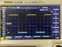
In the picture, it can be seen the blue trace rise step and in yellow the fall step. While the rise is fast and very sharp, the fall is not. No matter the compensation caps, I was unable to substantially improve the behavior. I am suspecting the flattening behavior on the fall trace here, might be an artifact of the limiting sampling, I might double check the behavior with the 350MHz Tek analog scope.
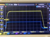
Also to show the signal generator fall behavior, below, yellow trace is the same as above (output of the buffer) while in blue is the signal generator. This can help assess the behavior of the fuffer.
Last, I don't have a scope shot to post here, but If I feed the input with a 3MHz or more sine, the output starts distorting/sagging greatly.
I am wondering the following things, if you can point me out I would great appreciate it:
1) Have detailed measurements on a physical prototype even been made and posted? (step response, distortion, frequency response)
2) Is it possible to buy a production Calvin Buffer somewhere so I can make a full set of measurements?
Thank you!
P.S. if you are reading this post, could you please share your thoughts? @Calvin .Thank you.
You can avoid the problem with the cap in the White follower by changing to the Taylor source follower.
https://www.tubecad.com/2004/blog0023.htm
https://www.diyaudio.com/community/...a-zgf-headphone-amplifier.225577/post-3297425
Patrick
https://www.tubecad.com/2004/blog0023.htm
https://www.diyaudio.com/community/...a-zgf-headphone-amplifier.225577/post-3297425
Patrick
I did already, right after the first time you suggested it to me, but no answer so far unfortunately.Why not try to PM him ?
Patrick
I don't understand this.I don't use fancy shunt regulators for every circuit.
Actually I don't use them at all.
We have had huge oscillations with the F5 headamp with some shunt regulators.
Change to simple cap multiplier, everything is fine.
Different regulators have different frequency response and stability with complex load.
Patrick
In usual used serial regulators there is between the main capacitor and the voltage rails the serial regulator itself - and a small capacitance behind it - mostly between 10uF and 47uF.
This small capacitors does not completely eliminate the sound signature of the serial regulator independent of the fact, if there is an integrated or discrete variant.
For me a parallel regulator resp. shunt regulator provide the great advantage, that the large main capacitor is located directly between pos. and neg. rail of the amplifier resp. buffer stage. Actually we have the same topology as to find with supply voltage by accu, which will be recharge by a constant current source (CCS) from time to time.
In post #8 (first PDF) under
https://www.diyaudio.com/community/...etween-mark-levinsons-jc-1-and-jc-1dc.243267/
you will find my solution for such a charger (for Mark Levinson's JC-1DC) - where the accu is replace by several big capacitors in parallel mode.
The provided current in the 3V zener diode - which consist of discrete parts - has twice the value of the current that the JC-1DC draws.
Sonic performance is better in all respects compare to a usual serial regulator and even to capacitance multiplier consist of a transistor, resistor and capacitors on base and emitter.
Check out also this thread:
https://www.diyaudio.com/community/threads/questions-about-shunt-regs.309096/
Please let me know more about your used circuit of your shunt regulator for your F5 (first watt series) which provide unexpected issues concerning unwanted oscillation (ring-ring).
The article in Linear Article on regulator shootout has rather different conclusions.
But we are both free to choose what we want.
No need to impose anything on someone else.
Cheers,
Patrick
But we are both free to choose what we want.
No need to impose anything on someone else.
Cheers,
Patrick
Personally, I have implemented from basic series regulator to more advanced Jung regulator and shunt as well. To me they all sound slightly different. I wouldn't say one is completely better than another. It depends on the application and also the sonic signature you trying to achieve.I don't understand this.
In usual used serial regulators there is between the main capacitor and the voltage rails the serial regulator itself - and a small capacitance behind it - mostly between 10uF and 47uF.
This small capacitors does not completely eliminate the sound signature of the serial regulator independent of the fact, if there is an integrated or discrete variant.
For me a parallel regulator resp. shunt regulator provide the great advantage, that the large main capacitor is located directly between pos. and neg. rail of the amplifier resp. buffer stage. Actually we have the same topology as to find with supply voltage by accu, which will be recharge by a constant current source (CCS) from time to time.
In post #8 (first PDF) under
https://www.diyaudio.com/community/...etween-mark-levinsons-jc-1-and-jc-1dc.243267/
you will find my solution for such a charger (for Mark Levinson's JC-1DC) - where the accu is replace by several big capacitors in parallel mode.
The provided current in the 3V zener diode - which consist of discrete parts - has twice the value of the current that the JC-1DC draws.
Sonic performance is better in all respects compare to a usual serial regulator and even to capacitance multiplier consist of a transistor, resistor and capacitors on base and emitter.
Check out also this thread:
https://www.diyaudio.com/community/threads/questions-about-shunt-regs.309096/
Please let me know more about your used circuit of your shunt regulator for your F5 (first watt series) which provide unexpected issues concerning unwanted oscillation (ring-ring).
Myself, I prefer shunt regulators on preamps, and series regulator on FE of power amps, but again it depends on what circuit you are using them in.
There is no fits all solution, you need to try and decide for yourelf.
Are you suggesting changing topology and switch to the Taylor current source configuration?You can avoid the problem with the cap in the White follower by changing to the Taylor source follower.
https://www.tubecad.com/2004/blog0023.htm
https://www.diyaudio.com/community/...a-zgf-headphone-amplifier.225577/post-3297425
Patrick
Would you mind just explain a bit further?
Thank you, Patrick! If I understand correctly, you are suggesting using the design below, in place of the calvin buffer I have implemented:

My problem here is that PCB boards have been manufactured already and converting the buffer would be a multitude of cuts and jumps.
If I was more diligent I would have prototyped, carefully measured different buffers.
In the past, I have used the calvin buffer on a one stage Phono with current RIAA and had no issue, but of couse, I didn't look closely at any square wave response.
At this point, I am still questioning, if it is my implementation that has those flaws. since so many people have participated on the Calvin design and I am sure they have taken detailed measurements.
I would like to fix the response. I am observing by touching J13 i.e. introducing capacitance, the fall response changes, which means there is some instability within the buffer.
I tried to increase the gate stopper resistors, but it had no impact on it, Changed C129, C130 values but I have to remove them off completely or else the response worsens dramatically.

The circuit simulates great, so I am not sure why I am getting such a problem with this implementation!
My problem here is that PCB boards have been manufactured already and converting the buffer would be a multitude of cuts and jumps.
If I was more diligent I would have prototyped, carefully measured different buffers.
In the past, I have used the calvin buffer on a one stage Phono with current RIAA and had no issue, but of couse, I didn't look closely at any square wave response.
At this point, I am still questioning, if it is my implementation that has those flaws. since so many people have participated on the Calvin design and I am sure they have taken detailed measurements.
I would like to fix the response. I am observing by touching J13 i.e. introducing capacitance, the fall response changes, which means there is some instability within the buffer.
I tried to increase the gate stopper resistors, but it had no impact on it, Changed C129, C130 values but I have to remove them off completely or else the response worsens dramatically.
The circuit simulates great, so I am not sure why I am getting such a problem with this implementation!
I looked around for everything related to the Calvin buffer, and I came across one scope shot taken by @Joachim Gerhard that has the same behavior as mine.

I will take few more measurements tonight and post, including the modulated version and unmodulated (with no bootstrap capacitor
C46).
I will take few more measurements tonight and post, including the modulated version and unmodulated (with no bootstrap capacitor
C46).
Hi Stefanoo,
please remember this is a buffer designed for audio output. Your scope shots show its behaviour for a high-speed square wave signal. With a rising input, the upper half of the circuit operates as a strong pull-up (with the combined gain of the JFET and the PNP) against the current source of the lower half, while at falling input the upper current source shuts down against the current source of the lower half.
So, as you move out of small-signal domain and into large-signal, the behaviour you show will become obvious: Output rising edge really sharp, output falling edge proportional to bias current and output capacitance (including the internal capacitances of the circuit elements, of course). Your first scope shots shows a fall time of ~200ns or 3dB bandwidth of ~5MHz (falling edge) while the rising edge is much faster.
Joachim's scope shot shows a 10kHz square wave, and - with "usual" cable capacitance at the output - should be just perfect. I wouldn't read too much into a few unclear pixels....
Getting more and more motivated to build a couple and measure myself 😀 To my shame, I must confess I sold my Paradise to a friend who is very very happy with it....
I agree with your findings. Building shunt regulators for high current (power amps) is difficult, as the power devices have a lot of transconductance at nominal current and that gain is heavy for the control loop.Personally, I have implemented from basic series regulator to more advanced Jung regulator and shunt as well. To me they all sound slightly different. I wouldn't say one is completely better than another. It depends on the application and also the sonic signature you trying to achieve.
Myself, I prefer shunt regulators on preamps, and series regulator on FE of power amps, but again it depends on what circuit you are using them in.
There is no fits all solution, you need to try and decide for yourelf.
In the Paradise, we had a nice number of shunt regulator issues, for two main reasons (wrong LED polarity and oscillations). The oscillations were mostly due to people swapping parts, or getting a batch of transistors with unexpectedly high beta.
From playing with shunt regulators in other (preamp) designs, I get the feeling that they can be very nervous animals if the load is off, both in simulation as well as testing. But when they work correctly, they are wonderful! (provided their corner frequency for the regulation loop is outside the audio band). I could compare both the Paradise as well as a tube preamp with/without shunt and the difference was very clear.
Hi Hesener,Hi Stefanoo,
please remember this is a buffer designed for audio output. Your scope shots show its behaviour for a high-speed square wave signal. With a rising input, the upper half of the circuit operates as a strong pull-up (with the combined gain of the JFET and the PNP) against the current source of the lower half, while at falling input the upper current source shuts down against the current source of the lower half.
So, as you move out of small-signal domain and into large-signal, the behaviour you show will become obvious: Output rising edge really sharp, output falling edge proportional to bias current and output capacitance (including the internal capacitances of the circuit elements, of course). Your first scope shots shows a fall time of ~200ns or 3dB bandwidth of ~5MHz (falling edge) while the rising edge is much faster.
Joachim's scope shot shows a 10kHz square wave, and - with "usual" cable capacitance at the output - should be just perfect. I wouldn't read too much into a few unclear pixels....
Getting more and more motivated to build a couple and measure myself 😀 To my shame, I must confess I sold my Paradise to a friend who is very very happy with it....
Yes, you are correct, BW is greater than 5MHz (here I am using the 5MHz GwInstek signal gen, I will use my other 50MHz Tek generator to establish the exact bandwidth I suspect it is roughly 7-).
You are also correct with the fact that rising and falling edges are depending on grounding and capacitance of probe and anything else connected, so those behaviors have to be taken with a grain of salt.
However, it seems consistent i.e. not an artifact, to see an increasing falling undershoot as the input/output signal grows.
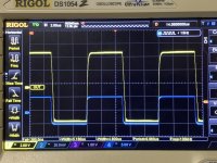
As it can see, the transient response at 4.5Vpp level is "perfect"
However, as the voltage increases over 5Vpp, the undershoot starts becoming obvious:
I haven't taken pictures, but as the voltage keeps increasing the undershoot will dramatically grow. I tried everything to get rid of this behavior but without any success. I also, have tried the unmodulated configuration, but the behavior doesn't change,
The scope shot from @Joachim Gerhard shows roughly 20Vpp, however in my measurements, this phenomenon shows up much earlier, and I am not sure why this large discrepancy. In my case the supply is +/-24V, 25-30mA biasing and no load at the output.
While in any practical use, signals don't have this transient and driving a power amp, depending on sensitivity, but average, 2-3VRMS will usually equal to max output power, still from an ideal technical perspective, we would like to see a perfect square wave at least 50-60% of the rail.
I would be real interested to match your measurements. Too bad you have sold your paradise 🙂 ...or better.......good you sold it to someone that can put it to good use......just in case you need boards to build to measure the buffer @curryman should still have few PCBs left.
I was hoping for some inputs also from the people who took active part to this project, however they went mute 🙂
If you build one proto I would be very interested to compare results as at this point, I am scratching my head thinking what can be done to improve.
P.S. the latest scope shots use the Toshibas 2SA1837 which seems to offer slightly better stability overall.
Shunt regulators are tricky to build stable I agree, not for everyone, but I do agree that on preamplifiers, they provide a more refined sound with clearer image and a bit more depth and definition of the different layers of sound.I agree with your findings. Building shunt regulators for high current (power amps) is difficult, as the power devices have a lot of transconductance at nominal current and that gain is heavy for the control loop.
In the Paradise, we had a nice number of shunt regulator issues, for two main reasons (wrong LED polarity and oscillations). The oscillations were mostly due to people swapping parts, or getting a batch of transistors with unexpectedly high beta.
From playing with shunt regulators in other (preamp) designs, I get the feeling that they can be very nervous animals if the load is off, both in simulation as well as testing. But when they work correctly, they are wonderful! (provided their corner frequency for the regulation loop is outside the audio band). I could compare both the Paradise as well as a tube preamp with/without shunt and the difference was very clear.
Hello Stefanoo, as requested per PM. Please find measurements below.
Load is 47K metalfilm.
I see similar findings as you at 100Khz. Remember, we are talking audio here 😉
Load is 47K metalfilm.
I see similar findings as you at 100Khz. Remember, we are talking audio here 😉
Attachments

Bensen,
First of all, I want to thank you for taking the time to measure this for me. I do appreciate it very much!!
In reviewing your results, I can see some significant differences with mine:
1) the total gain of your circuit is much higher than in mine (I have 11dB gain).
Do you have the buffer in a closed loop with the VAS /Input stage or is it outside of the loop?
2) your fall time is about 1us, which is much slower than in my case (I have around 200-250ns fall time), but to be expected given you have a much higher gain.
Do you have zobel network at the output? If so, do you know how is the response before the filter?
3) very important, in your case, you have the undershoot at a very high voltage output, in my case, this happens at 2-3Vpp while in your case at 20Vpp which is significantly better.
What rail voltage and output bias do you have for the buffer? I have +/-24V 30mA.
I will take scope shots at higher output level to render the issue I am facing clearer.
Would you mind sharing the devices/values you are using in the buffer and what compensation cap values you have installed?
Thank you.
Stefano.
- Home
- Amplifiers
- Solid State
- Calvin buffer large inrush current