3.3V I2S attenuator & DEM-Reclock changes
If we look to the calculated pull up and pull down voltages for 3.3V in the I2S attenuator that John stated,
i came to the conclusion that we need a 200R series, 62R pull up and 47R pull down resistor to get an adequate voltage level for BCK.
But this is only theoretical...🙄
The next question goes to the DEM reclock and the 10K (12K with series diodes) resistor value. Must this also be lowered for a 3.3V BCK signal?
@ John
Could you please look to my calculation and the DEM resistor question.
Thank´s in advance.
Oliver

Thanks for this..
I'm a little confused because if the source impedance is the parallel value of the three resistors, consider the values of both WS and DATA 3k3//3k3//1k = 622ohms in the 5V attenuator cct, and 1k//1k//680 = 288 ohm in the 3v3 attenuator cct.
However, the values for WS and DATA have been given, and just BCK remains unknown (to me anyway). If I use the given values for the 5V cct 500//68//220 = ~47ohms.
If the attenuation is a function of the voltage divider created by the series resistor and the shunt resistor to ground, then signal level for WS and DATA in the 5V cct, after the divider, is 1.1V (this is Vpp?) and only 0.59V for BCK?.
If its desirable to have amplitude of the three lines between 1.2 and 1.4Vpp, and each biased between 1 and 1.4V, with a parallel resistor value of ~50 ohms for BCK, then the values I've arrived at are as in the attached image.
Does this all seem correct, or at least correct enough for the purpose, or have I got it all backwards?🙄
Thanks,
Shane
If we look to the calculated pull up and pull down voltages for 3.3V in the I2S attenuator that John stated,
An externally hosted image should be here but it was not working when we last tested it.
i came to the conclusion that we need a 200R series, 62R pull up and 47R pull down resistor to get an adequate voltage level for BCK.
But this is only theoretical...🙄
The next question goes to the DEM reclock and the 10K (12K with series diodes) resistor value. Must this also be lowered for a 3.3V BCK signal?
@ John
Could you please look to my calculation and the DEM resistor question.
Thank´s in advance.
Oliver
Oliver
Wouldn´t the +5V still be +5V and not 3,3V as this is part of the PS for TDA1541A.
Otherwise you would have to make chages to the pcb ?
Koldby
Wouldn´t the +5V still be +5V and not 3,3V as this is part of the PS for TDA1541A.
Otherwise you would have to make chages to the pcb ?
Koldby
Oliver
Wouldn´t the +5V still be +5V and not 3,3V as this is part of the PS for TDA1541A.
Otherwise you would have to make chages to the pcb ?
Koldby
Hi Koldby,
a bit off topic here 😱 but anyway.
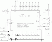
The I2S attenuator on the Red Baron get´s the voltage not from the +5V line of the TDA1541A, but from the separate voltage line of the DEM reclock IC.
With this independent voltage line, we could go to +3.3V without problems. The 74HC02 (DIP14) or the 74LVC1G02 (SOT323) runs with a Vcc of 3.3V.
Only small changes to the +5V Salas shunt module are necessary to get an output voltage of 3.3V. Look HERE. 😉
Hi dvb-project,
Sorry but I have been very busy developing the next generation SD-players together with my brother.
Back to your question,
The best TDA154x I2S attenuators for WS and DATA are circuits resembling the TDA154x I2S input circuit. You could try 3 x 1N4148 to GND (all cathodes facing GND), 1 x 1N4148 in series with WS / DATA input signal (cathode facing source), and 2K2 pull-up resistor to +3.3V. This would give a signal swing between +0.6V and + 1.8V, regardless of input signal level.
With some creativity you could fit these components on the existing PCB:
- Replace 3K3 resistors (attached to +3V3!) with 2K2 resistors (WS & DATA).
- Replace 1K resistors with diode string of 3 x 1N4148 in series (cathodes facing GND).
- Replace 3K3 resistors in series with WS & BCK with a diode (cathode facing digital audio source).
BCK is extremely critical, attenuators are best avoided here, even plain series resistors are a problem (noise). Best results can be achieved by using 800mVpp BCK signal (not derived from an attenuator) with less than approx. 300 Femto seconds of jitter, but this is kind of "problematic" 🙂
So simply remove the BCK attenuator and hope for the best:
- Remove 68R, 220R, 10mH choke and all 100 Ohm resistors. Feed source BCK signal directly to pin 2.
Synchronising the DEM oscillator remains extremely critical and performance is inconsistent and unpredictable due to thermal drift of the TDA1541A circuits and other factors.
I have some ideas about a suitable DEM synchroniser circuit, but for now I suggest to go for the low jitter, free-running DEM oscillator:
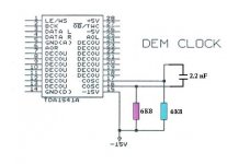
- Replace both 2K2 resistors with 6K8 resistors, remove both 10K resistors and the CMOS crap.
- Put a 2.2nF SMD film cap between pins 16 and 17 (as close as possible to the chip).
This means that there is no more external DEM oscillator triggering.
@ John
Could you please look to my calculation and the DEM resistor question.
Thank´s in advance.
Sorry but I have been very busy developing the next generation SD-players together with my brother.
Back to your question,
The best TDA154x I2S attenuators for WS and DATA are circuits resembling the TDA154x I2S input circuit. You could try 3 x 1N4148 to GND (all cathodes facing GND), 1 x 1N4148 in series with WS / DATA input signal (cathode facing source), and 2K2 pull-up resistor to +3.3V. This would give a signal swing between +0.6V and + 1.8V, regardless of input signal level.
With some creativity you could fit these components on the existing PCB:
- Replace 3K3 resistors (attached to +3V3!) with 2K2 resistors (WS & DATA).
- Replace 1K resistors with diode string of 3 x 1N4148 in series (cathodes facing GND).
- Replace 3K3 resistors in series with WS & BCK with a diode (cathode facing digital audio source).
BCK is extremely critical, attenuators are best avoided here, even plain series resistors are a problem (noise). Best results can be achieved by using 800mVpp BCK signal (not derived from an attenuator) with less than approx. 300 Femto seconds of jitter, but this is kind of "problematic" 🙂
So simply remove the BCK attenuator and hope for the best:
- Remove 68R, 220R, 10mH choke and all 100 Ohm resistors. Feed source BCK signal directly to pin 2.
Synchronising the DEM oscillator remains extremely critical and performance is inconsistent and unpredictable due to thermal drift of the TDA1541A circuits and other factors.
I have some ideas about a suitable DEM synchroniser circuit, but for now I suggest to go for the low jitter, free-running DEM oscillator:
- Replace both 2K2 resistors with 6K8 resistors, remove both 10K resistors and the CMOS crap.
- Put a 2.2nF SMD film cap between pins 16 and 17 (as close as possible to the chip).
This means that there is no more external DEM oscillator triggering.
Abeus Papam
Hi John, Nice to see you here again,🙂
Thank you for the DEM 2.2 nf value .
DO you have a shematic for the last clock you talked about (one crystal, two UHS buffer : can we use the MK7 shematic but with one crystal ?)
As noise has to be avoided, and a low voltage source has to be used for the clock and for IIS, is it possible to go with low voltage battery and a fast cap to powersupply the clock ? (less noiser than your shund shematic or not...and easier (?) for me in a DIY perspective)
For example 3,3 v battery with a ultra low ESR cap and a // film cap and a mini shunt for the power supply of the clock : it coul be ok for feeding the IIS clock source but how lowering 3,3 V to 0,8 V for the TDA' s BcK pin ? A divide by 4 with two SN74AUC1G74 is still good enough , but here without the 180R?
You talk about Zener in serie for WS & Data : active zener are less noisy than a good passive resistor like the bulky wirewound you talked about ? Too big for EMC ?
cheers
Last edited:
Hi dvb-project,
Synchronising the DEM oscillator remains extremely critical and performance is inconsistent and unpredictable due to thermal drift of the TDA1541A circuits and other factors.
I have some ideas about a suitable DEM synchroniser circuit, but for now I suggest to go for the low jitter, free-running DEM oscillator:
- Replace both 2K2 resistors with 6K8 resistors, remove both 10K resistors and the CMOS crap.
- Put a 2.2nF SMD film cap between pins 16 and 17 (as close as possible to the chip).
This means that there is no more external DEM oscillator triggering.
Hi
I'm using this DEM synchroniser circuit from Grunding.
Is it better to replace it by your suggestion of using 6K8 resistors, no cmos, and 2.2nF SMD film cap between pins 16 and 17, like in my second image ?
Thanx
Paul
Attachments
Last edited:
John, good to see you back. Have been following some results of your effort with the tda1543 on another Dutch website.
Just wanted to note that without inline resistors I am experiencing significant overshoot on bck coming from the Johnson counter flip flops...
BCK is extremely critical, attenuators are best avoided here, even plain series resistors are a problem (noise). Best results can be achieved by using 800mVpp BCK signal (not derived from an attenuator) with less than approx. 300 Femto seconds of jitter, but this is kind of "problematic" 🙂
Just wanted to note that without inline resistors I am experiencing significant overshoot on bck coming from the Johnson counter flip flops...
Hi dvb-project,
Sorry but I have been very busy developing the next generation SD-players together with my brother.
Back to your question,
The best TDA154x I2S attenuators for WS and DATA are circuits resembling the TDA154x I2S input circuit. You could try 3 x 1N4148 to GND (all cathodes facing GND), 1 x 1N4148 in series with WS / DATA input signal (cathode facing source), and 2K2 pull-up resistor to +3.3V. This would give a signal swing between +0.6V and + 1.8V, regardless of input signal level.
With some creativity you could fit these components on the existing PCB:
- Replace 3K3 resistors (attached to +3V3!) with 2K2 resistors (WS & DATA).
- Replace 1K resistors with diode string of 3 x 1N4148 in series (cathodes facing GND).
- Replace 3K3 resistors in series with WS & BCK with a diode (cathode facing digital audio source).
BCK is extremely critical, attenuators are best avoided here, even plain series resistors are a problem (noise). Best results can be achieved by using 800mVpp BCK signal (not derived from an attenuator) with less than approx. 300 Femto seconds of jitter, but this is kind of "problematic" 🙂
So simply remove the BCK attenuator and hope for the best:
- Remove 68R, 220R, 10mH choke and all 100 Ohm resistors. Feed source BCK signal directly to pin 2.
Synchronising the DEM oscillator remains extremely critical and performance is inconsistent and unpredictable due to thermal drift of the TDA1541A circuits and other factors.
I have some ideas about a suitable DEM synchroniser circuit, but for now I suggest to go for the low jitter, free-running DEM oscillator:
- Replace both 2K2 resistors with 6K8 resistors, remove both 10K resistors and the CMOS crap.
- Put a 2.2nF SMD film cap between pins 16 and 17 (as close as possible to the chip).
This means that there is no more external DEM oscillator triggering.
Thanks John!
I will build it up on a new RB module to test your recommendations.
Cheers,
Oliver
You guys are the best.
I'd like to ask why not bias BCK above zero volt even if not using attenuation.
Thanks (alot)
Shane
I'd like to ask why not bias BCK above zero volt even if not using attenuation.
Thanks (alot)
Shane
Of course 🙄Hi Koldby,
a bit off topic here 😱 but anyway.
The I2S attenuator on the Red Baron get´s the voltage not from the +5V line of the TDA1541A, but from the separate voltage line of the DEM reclock IC.
With this independent voltage line, we could go to +3.3V without problems. The 74HC02 (DIP14) or the 74LVC1G02 (SOT323) runs with a Vcc of 3.3V.
Only small changes to the +5V Salas shunt module are necessary to get an output voltage of 3.3V. Look HERE. 😉
Didn´t see that at first, sorry.
Thanks Oliver.
Koldby
Have been following some results of your effort with the tda1543 on another Dutch website.
Hi, could you post the link to this Dutch website, maybe interesting for all of us.
Where in the site? I can't find it
Thanks John!
I will build it up on a new RB module to test your recommendations.
Cheers,
Oliver
Maybe with u. fl inputs as well?......
Thanks John!
I will build it up on a new RB module to test your recommendations.
Cheers,
Oliver
.. and free running DEM option if possible
I2S Attenuator for 3.3V and free run DEM Clock
@ John
For a quick verification if everything is correct! 🙄
Doei,
Oliver
@ John
For a quick verification if everything is correct! 🙄
An externally hosted image should be here but it was not working when we last tested it.
Doei,
Oliver
Hey John,
You used pin recepticals for the 1541 on an earlier version of your DAC (v1.3?)
Do you have a part number or specs for these recepticals that fit the 1541 pins?
Thanks,
Jeff
You used pin recepticals for the 1541 on an earlier version of your DAC (v1.3?)
Do you have a part number or specs for these recepticals that fit the 1541 pins?
Thanks,
Jeff
Oliver,
Are you thinking to use your 3.3V shunt for the attenuation voltage?
Also...might you consider another set of "holes" parallel to C1 for those of us that "might" want to run a different value cap plus an air cap?
I'm excited to see what you come up with!
Are you thinking to use your 3.3V shunt for the attenuation voltage?
Also...might you consider another set of "holes" parallel to C1 for those of us that "might" want to run a different value cap plus an air cap?
I'm excited to see what you come up with!
Hi Chris,
Definitive yes!
I will keep it in mind 😉
First i will build up Johns recommendations on a blank Red Baron to see if everything work well and to make some photos of the changes for those, who want to use Ian´s FIFO.
Are you thinking to use your 3.3V shunt for the attenuation voltage?
Definitive yes!
Also...might you consider another set of "holes" parallel to C1 for those of us that "might" want to run a different value cap plus an air cap?
I will keep it in mind 😉
First i will build up Johns recommendations on a blank Red Baron to see if everything work well and to make some photos of the changes for those, who want to use Ian´s FIFO.
Where in the site? I can't find it
http://www.kadmeia.nl/pages/sub/12/SDdac_in_werking.html
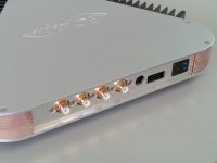
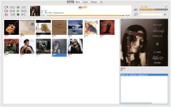
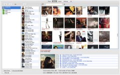
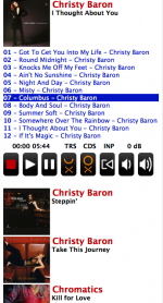
I attached some pictures of the SDV1-player that was just completed. Here the separate SD-player and volume control units are integrated in one housing.
I also added some screenshots of the matching computer software, the SD(V)1 can be (wirelessly) controlled by computer, laptop, pad, or smartphone.
The new SD-player supports up to 999 CDs on one single SDXC card, it runs on an external 12V power source, mains adapter, battery, solar cell ...
Attachments
- Home
- Source & Line
- Digital Line Level
- Building the ultimate NOS DAC using TDA1541A