Charge Transfer PS
ec-designs,
Excellent idea that you have in the charge transfer PS.
A few questions if I may:
1. Lets assume I have a "normal" PS: transformer, bridge diode (full wave), smoothing caps.
Could I simply cut the link between the bridge diode and the smoothing cap and insert R1, R2, R3, D5, T1, D3, D4 and R4? Would this provide the same benefit in terms of cleaner power supply?
2. Could I use other MOSFETS instead of 2SJ380? What is the important parameter when selecting the MOSFET?
3. Is it critical that D3, D4 be 11DQ10? Can I use ANY diode in this place?
4. What about D5 (BAT42)? Could it be something else? What is the parameter to select the diode for that position?
Thanks and great work!
Ryan
hi MGH
thanks for your reply
hi ecdesigns
I'm very interest for your DI-DAC
can you help me?
I want to use TDA1545A more than TDA1543 for the DI-DAC
best regard
sam
thanks for your reply
hi ecdesigns
I'm very interest for your DI-DAC
can you help me?
I want to use TDA1545A more than TDA1543 for the DI-DAC
best regard
sam
May be Vacation this year?
Well, we seem to be entering a very hot and sunny summer (for the second year) here in the south of Chile. Consider both of you invited to my humble residence 🙂 if you feel the need to escape the winter rigors.
http://www.adn.es/clipping/ADNIMA20080218_2401/4.jpg
http://www.fotopaises.com/imagenes/2007/11/4/4618_1194212687.jpg
http://img117.imageshack.us/img117/5575/2138533617d95d72a2fcbfk8.jpg
(don-t forget to bring your own iron)

Cheers,
M
Hi Dr.H,
First check the required current, the posted circuit is rated for approx. 250 ... 300mA.
Yes that should be possible, provided total voltage drop isn't too high, the charge-transfer circuit has a typical voltage drop of approx. 2 volts. The capacitor multiplier is added to reduce ripple voltage to very low values prior to feeding the voltage regulators. This is very important when using local voltage regulators.
Yes, you can use other MOSFETs, best select on low Vgs threshold voltage and low Rdson. Also check if the MOSFET has internal protection diodes, if not, these should be added externally.
Schottky rectifier diodes were used to reduce switching noise (property of Schottky diodes) and the advantage of the lower voltage drop. It's also possible to use suitable silicon diodes (fast-slow recovery). D4 was added to reduce the effects of the relatively high output and transfer capacitance of the MOSFET, the 11DQ10 has relatively low capacitance, larger Schottky diodes have higher capacitance and are less suitable here. Allowing large capacitance between both source and cathode of D4 will leave a path for power supply HF interference (HF passes both MOSFET and D4, even if the MOSFET doesn't conduct).
I used a Schottky diode here because of low switching noise, but silicon diodes like the 1N4148 should work too. The function of this diode is to switch-off the gate fast through 100K (R1) to prevent the MOSFET from conducting when C1 starts charging, and switch-on slowly through R3, R1, and R2 (1.11M Ohm) to limit surge currents during charge-transfer between both C1 and C2.
First check the required current, the posted circuit is rated for approx. 250 ... 300mA.
Could I simply cut the link between the bridge diode and the smoothing cap and insert R1, R2, R3, D5, T1, D3, D4 and R4? Would this provide the same benefit in terms of cleaner power supply?
Yes that should be possible, provided total voltage drop isn't too high, the charge-transfer circuit has a typical voltage drop of approx. 2 volts. The capacitor multiplier is added to reduce ripple voltage to very low values prior to feeding the voltage regulators. This is very important when using local voltage regulators.
Could I use other MOSFETS instead of 2SJ380? What is the important parameter when selecting the MOSFET?
Yes, you can use other MOSFETs, best select on low Vgs threshold voltage and low Rdson. Also check if the MOSFET has internal protection diodes, if not, these should be added externally.
Is it critical that D3, D4 be 11DQ10? Can I use ANY diode in this place?
Schottky rectifier diodes were used to reduce switching noise (property of Schottky diodes) and the advantage of the lower voltage drop. It's also possible to use suitable silicon diodes (fast-slow recovery). D4 was added to reduce the effects of the relatively high output and transfer capacitance of the MOSFET, the 11DQ10 has relatively low capacitance, larger Schottky diodes have higher capacitance and are less suitable here. Allowing large capacitance between both source and cathode of D4 will leave a path for power supply HF interference (HF passes both MOSFET and D4, even if the MOSFET doesn't conduct).
What about D5 (BAT42)? Could it be something else? What is the parameter to select the diode for that position?
I used a Schottky diode here because of low switching noise, but silicon diodes like the 1N4148 should work too. The function of this diode is to switch-off the gate fast through 100K (R1) to prevent the MOSFET from conducting when C1 starts charging, and switch-on slowly through R3, R1, and R2 (1.11M Ohm) to limit surge currents during charge-transfer between both C1 and C2.
Hi sam27,
If I am correct the TDA1545A uses the EIAJ protocol, so the existing 16 x interpolator won't work (glue logic required). It's also better to go for 4x interpolation instead of the 16x interpolation used in the DI16.
The DAC chips specs are important, but perceived sound quality is mainly determined by the surrounding circuits. Most DAC chips are capable of much higher performance when used in an optimized circuit.
I want to use TDA1545A more than TDA1543 for the DI-DAC
If I am correct the TDA1545A uses the EIAJ protocol, so the existing 16 x interpolator won't work (glue logic required). It's also better to go for 4x interpolation instead of the 16x interpolation used in the DI16.
The DAC chips specs are important, but perceived sound quality is mainly determined by the surrounding circuits. Most DAC chips are capable of much higher performance when used in an optimized circuit.
-ecdesigns- said:Hi Telstar,
Interpolation needs to be identical for both channels, so with 4 x mono PCM1704 for each channel, only 4 x DI can be achieved.
Thank you John. I wasn't actually sure.
Based on your experience, would you recommend 4x DI, regardless of the chip used? Or 8x could achieve better results?
The PCM1704 interface is also different from the TDA154X, and it's a mono DAC, this requires a complete re-design of the existing DI / scrambler circuit.
But it wouldnt require a redesign of every other circuits you made i guess 🙂
Hi ecdesigns
thanks for your reply
I'm favor a DI-DAC without LPF
can you post a time-chan sch for 4xTDA1545A?
best regard
sam
thanks for your reply
I'm favor a DI-DAC without LPF
can you post a time-chan sch for 4xTDA1545A?
best regard
sam
Hi Sam,
I'm sorry Sam, -EC- will be busy designing a 48*BCK timing chain/scrambler, for the CD PRO fans... 😀 😉
Regards,
M
Hi ecdesigns,
Can you post a time-chan sch for 4xTDA1545A?
I'm sorry Sam, -EC- will be busy designing a 48*BCK timing chain/scrambler, for the CD PRO fans... 😀 😉
Regards,
M
Hi Max
thanks for your reply
Is the 48BCK means the EIAJ protocol?
I will be happy and watting
(If you unknow what my post, that me too)
best regard
sam
🙂
thanks for your reply
Is the 48BCK means the EIAJ protocol?
I will be happy and watting
(If you unknow what my post, that me too)
best regard
sam
🙂
Hi Sam,
I'm afraid not. In this case we are talking I2S.
Quick googling:
http://www.freescale.com/files/dsp/...ALE&WT_FILE_FORMAT=pdf&WT_ASSET=Documentation
See section 4.
Cheers,
M
I'm afraid not. In this case we are talking I2S.
Quick googling:
http://www.freescale.com/files/dsp/...ALE&WT_FILE_FORMAT=pdf&WT_ASSET=Documentation
See section 4.
Cheers,
M
I wish you all a happy new year,
Have a look at diyAudio Forums > Top > Source > Digital > EIAJ to I2S and vice versa.
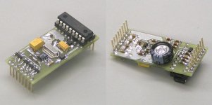
2009 started with some interesting new developments, a new module was designed, this module holds tracker, master clock, and clock buffers.
I attached a picture of this new module,
Picture on the left shows the component side, the micro controller is placed in an IC-socket. It wasn't possible to use an 8 or 14 pin Microchip controller because the timer #1 input pin shares the external clock input pin, and a separate clock and timer #1 input were needed.
At the front there are the 4 UHS clock buffers, they are connected to the master clock using 2 x 47 Ohm series resistors. The VCXO master clock is built around the WF10192 chip that is programmed to divide the master clock by 4, providing exactly 50% duty cycle. The power supplies of micro controller and master clock are separately filtered (LC filters).
Picture on the right shows the solder side, on the left there are 4 decoupling caps for the clock buffers. In the center is the dual varactor diode with surrounding components. The crystal runs on very low power (series resistors). The large supercap is used for the master clock power supply. Above the supercap is the low-series capacitance filter that filters the DAC output signal prior to feeding it to the varactors. Filter consists of 3 x 220K, 100nF to GND, another 3 x 220K, and another 100nF to GND. The small SOT23-5 SMD chip on the right is a 12-bit Microchip DAC with serial interface. The DAC is guaranteed monotonous (series resistor ladder with taps), and provides approx. 5V full-scale with a resolution of approx. 1.22mV.
The master clock frequency is corrected once, every 2 seconds. The micro controller has 2 seconds to measure the delta frequency between it's own clock (varying master clock), and the external clock, and perform calculations to estimate required correction factor. This basically means that the master clock should be within range after only one correction (regardless of the frequency difference between both source and master clock). Then fine-adjustments take place to maintain accurate tracking.
(sam)can you post a time-chan sch for 4xTDA1545A?
Have a look at diyAudio Forums > Top > Source > Digital > EIAJ to I2S and vice versa.
2009 started with some interesting new developments, a new module was designed, this module holds tracker, master clock, and clock buffers.
I attached a picture of this new module,
Picture on the left shows the component side, the micro controller is placed in an IC-socket. It wasn't possible to use an 8 or 14 pin Microchip controller because the timer #1 input pin shares the external clock input pin, and a separate clock and timer #1 input were needed.
At the front there are the 4 UHS clock buffers, they are connected to the master clock using 2 x 47 Ohm series resistors. The VCXO master clock is built around the WF10192 chip that is programmed to divide the master clock by 4, providing exactly 50% duty cycle. The power supplies of micro controller and master clock are separately filtered (LC filters).
Picture on the right shows the solder side, on the left there are 4 decoupling caps for the clock buffers. In the center is the dual varactor diode with surrounding components. The crystal runs on very low power (series resistors). The large supercap is used for the master clock power supply. Above the supercap is the low-series capacitance filter that filters the DAC output signal prior to feeding it to the varactors. Filter consists of 3 x 220K, 100nF to GND, another 3 x 220K, and another 100nF to GND. The small SOT23-5 SMD chip on the right is a 12-bit Microchip DAC with serial interface. The DAC is guaranteed monotonous (series resistor ladder with taps), and provides approx. 5V full-scale with a resolution of approx. 1.22mV.
The master clock frequency is corrected once, every 2 seconds. The micro controller has 2 seconds to measure the delta frequency between it's own clock (varying master clock), and the external clock, and perform calculations to estimate required correction factor. This basically means that the master clock should be within range after only one correction (regardless of the frequency difference between both source and master clock). Then fine-adjustments take place to maintain accurate tracking.
Attachments
I wish you all a happy new year,
Oh! Of course, a happy new year to you all...
I was too sleepy and busy yesterday to remember it...

Best wishes,
M
maxlorenz said:
Oh! Of course, a happy new year to you all...
I was too sleepy and busy yesterday to remember it...
Best wishes,
M
From me also:
Happy new year 2009 to all.
I was busy too these days moved to another living place.
Sound from Sonic resonators (with DI4T and rest of chain) is now even better because room is bigger than before.
And John thanks for everything.
Best wishes,
Bostjan 😉
Hi ECdesigns,
You charge/transfer PS might be the biggest step forward to reach the Ultimate performance NOS DAC...I have one DAC totally *chargetransfered* (digital and analog part) and another with the modded digital part, which includes USB module, timing chain and DAC chips. This together with my DIY OCC monocrystal copper Litz interconnects and speaker cables, plus a secret tweak that is dangerous to comment here 😀 made my primary system highly resolving and musical, with a transparency that make my other systems sound muddy...
Unfortunatelly I ran out of Mosfets. As soon as they arrive I will start modding all other PS-s, including my humble phono preamp 🙂
Gratefully yours,
M
Just a question about the charge transfer PSU : you say a low rdson mosfet is good, then you put a 2R resistor in series. Since mosfets with a higher rdson have lower capacitance (usually) would it make a difference to use (say) something with 0.5 ohm rdson but a low capacitance ?
Also in simulations I see that a resistor between source and grid (acting as a voltage divider) can soften the current pulse going through the mosfet.
Also in simulations I see that a resistor between source and grid (acting as a voltage divider) can soften the current pulse going through the mosfet.
Hi max,
thanks for your reply
Does left and rignt analog signal came out from DAC at same time?or left channel first?
best regard
sam
thanks for your reply
Does left and rignt analog signal came out from DAC at same time?or left channel first?
best regard
sam
As far as I understand, the analog outputs L/R are simultaneous as long as there is info to output...a mono recording or a test signal should show this.
- Home
- Source & Line
- Digital Line Level
- Building the ultimate NOS DAC using TDA1541A