Rfbrw, I have used the TDA1543A with 32 bit subframe, right justified 24 bit data and it worked ok.
I haven´t checked each bit with oscilloscope. I wanted to check single bits toggling, anybody have wave files for that? At 88.2KHz preferably 🙂
-Alex
NOS no doubt. It violates timing at 4x. Then again you can violate timing with the TDA1541A. Still I wouldn't recommend going into production.
Rfbrw, you are correct, TDA1543A did not work correctly at 88.2. I just remembered that I was stuck with 44.1 when I was using it.
-Alex
-Alex
Hi Alexandre,
Here is the TDA1543A datasheet,
(Datasheet) TDA1543A pdf - Dual 16-bit DAC
Max. supported sample rate with 48 bits / frame equals 9.2 MHz / 48 = 191 KHz.
Max. supported sample rate with 64 bits / frame equals 9.2 MHz / 64 = 143 KHz.
So 88.2 and 96 KHz should work fine (bit clock frequency within specs), provided suitable glue logic is used.
When using glue logic that also offers clock rate conversion, it should be possible to have I2S (64 bits/frame) input and run TDA1543A at 4 times oversampling.
John, maybe there was something wrong with my setup, too large series resistors perhaps. But I do remember encountering problems trying to run it at 88.2 with 32 bit subframe.
I only have 3 units of the TDA1543A, bought them from a local vendor to run some tests. One good thing is it doesn´t have the skew between channels that the TDA1543 has.
One of the A's has perfect channel matching, I was able to fully cancel the sound by sending the same data to both channels and connecting differentially to my usual amp (similar to the one below but fully differential).
GC SuperSymmetry
That was, naturally, a good candidate for a differential/balanced dac. So I auditioned the one with perfect matching both diferentially and with channels in parallel, and the sound was definitely better with paralleled channels. I used passive I/V going to V+ rather than GND, and pin 7 open. Some digital attenuation assures that the voltage at the output stays under (V-1.2). I halved the resistor value when channels were paralleled and added R to balance impedance going to the amp.
I have better sonic results with the normal tda1543 and stopped clock. Especially at 88.2, which for me is a must.
-Alex
Hello everyone. Do you want to be supported by TDA1541(A) 192Khz? - consider this project: DAC na TDA1541(A) + AD1896 - DIY - Audiostereo.pl I'm not the author but I use and recommend it. Regards
Dear Alexandre, rfbrw and John,
Thanks for your inputs.
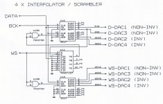
John, I've been revisiting the "scrambler-interpolator" DAC. It worked OK with 4 towers of 4 chips each. When I doubled 😀 the number of chips to 4 towers of 8 chips, it refused to work. I am investigating why today.
I presume that the CD4517 shift registers have too low current output to ride all those chips. If so, maybe I can piggy-back them 🙂 is it possible?
When I get it working, I will also do the "low thermal memory" mod AKA cascoded-CFP differential input for the diffamp out. 😎
Cheers,
M.
Thanks for your inputs.
John, I've been revisiting the "scrambler-interpolator" DAC. It worked OK with 4 towers of 4 chips each. When I doubled 😀 the number of chips to 4 towers of 8 chips, it refused to work. I am investigating why today.
I presume that the CD4517 shift registers have too low current output to ride all those chips. If so, maybe I can piggy-back them 🙂 is it possible?
When I get it working, I will also do the "low thermal memory" mod AKA cascoded-CFP differential input for the diffamp out. 😎
Cheers,
M.
Attachments
In an earlier answer to a similar question you wrote:Hi koldby,
TDA1543 has fixed I2S interface so it can't receive two data streams simultaneously.
We could modify the signed magnitude decoder so it outputs two I2S streams instead of 4 separate data streams, one for each TDA1543. This has the disadvantage that we always have trigger uncertainty due to digital interface activity and related crosstalk and ground-bounce during output latching.
But we could also apply quasi simultaneous mode, this would require 4 x TDA1543 and only a slight modification to the existing decoder
Quasi simultaneous mode:
- clock in R channel data while WS = 1 (we can only use the R channel / segment).
- Shut down interface (BCK and data) and wait for WS to go low.
- Wait another 16 bits and then latch the outputs with one extra pulse (LE) on BCK when ground-bounce and crosstalk have reached zero.
TDA1543A latches its outputs on the first rising edge of BCK after WS has gone low. If this single BCK pulse is delayed we can change the exact moment of output latching. This is only possible when we do not use the L channel.
It makes a lot of sense to operate the TDA1543 in segmented mode as this would eliminate the audibility of MSB related bit errors (big problem with the TDA1543) in this zero crossing region.
TDA1543 chips are not graded so you will have chips with high accuracy, chips that perform good, chips that perform too badly to be of any practical use and few that will be defective.
Roughly 5% of a larger batch (100+) of TDA1543 chips will perform pretty good and will have good channel matching.
Similar to the TDA1541, the TDA1543 transistors will need to have the same temperature for optimal accuracy (emitter scaling). This usually requires a warm-up period of at least half an hour or longer. This means that the chip will produce higher distortion (and related poorer sound quality) during this warm-up period.
The mentioned double zero code is corrected by ensuring that bit 15 of each segment (each represents 0.5 LSB in a segmented DAC) follows the MSB. This effectively adds one LSB, only when MSB = 1.
Originally Posted by ecdesigns View Post
L channel DATA is clocked in R input register of TDA1543 #1.
R channel DATA is clocked in R input register of TDA1543 #2.
So all L & R data is clocked in with 16 clock pulses when WS is “1”. Only the Right channel of each TDA1543 can hold data as DATA can only be clocked in when WS = "1".
Then BCK and DATA signals are shut down completely (total switching silence on the chip). Since I am only feeding clock signals to both TDA1543 chips during 16 of the available 64 pulses I reduce average switching noise levels by 75%.
In order to latch the outputs of both TDA1543 chips I multiplex a LE signal on BCK that produces a single LE transient after WS has gone low.
So the BCK input of both TDA1543 chips acts as both, BCK and LE input. This all is within the permissible specs of I2S.
By reducing on-chip switching noise by 75%, on-chip jitter levels are also reduced.
This requires a suitable I2S to quasi simultaneous mode converter. L & R signal data needs to be lined up too, this requires some shift registers.
As I see it you need 17 clock pulses and not 16 for the 1543 as it expects I2S format so the data must start 1 bitclock after WS goes high. So I think it would be better to design it from scratch as you are using some of the the glue logic to ensure the data starts when WS goes high in the I2S to Simultaious for the TDA1541. It would actually be easier I think.
Please correct me if I am wrong
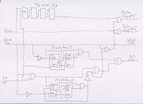
Could something like the attached work?
The AND gate low left puts out clk only when WS is high . The lowest 2 74xxx4017 (i love johnson counters 😉) selects the first 17 clk pulsesand puts them out to the x-or gate rightmost. The upper 74xxx4017 selects 1 clk pulse after WS is low and the x-or gate combines this with the 17 clk pulses .This is the LE for the two TDA1543.
The four 74xxx164 delays the left data 32 bits so it is synchronous with the right data.
There are probably a lot of errors in this, I am definitely not an expert in this kind of work, so please be kind😛
Attachments
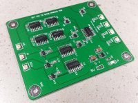
I2S to Simultaneous PCB
I've just completed the I2S to Simultaneous PCB based on ecdesigns schematics #6315
Tonight she sang, and without any hiccups when first powering it up - which is was a pleasant surprise.
I scraped the 4 layer idea to save on cost - its a lot more expensive to do small runs in 4 layers than 2 layers. So I re-designed it as a 2 layer.
Power consumption was surprisingly low at about 5mA so I have it powered by 4 NiMH cells which should give about 350 hrs of run time.
...oh, and its sounding pretty darn good too!
Attachments
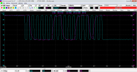
That is correct! Here´s mine. WS not shown, it goes high with the first bitclock high-to-low.As I see it you need 17 clock pulses and not 16 for the 1543 as it expects I2S format so the data must start 1 bitclock after WS goes high.
The first bit is the LSB of the left channel. In my case it will always be 1.
Then we have 16 bits of right channel. WS goes low after lhe LSB.
Then a single low to high transition of BCK triggers conversion on the right channel. In the middle of the "silence" preferably.
(I suppose I have to try the diodes now, to limit the swing to 1.8 volts.)
-Alex
Attachments
That is correct! Here´s mine. WS not shown, it goes high with the first bitclock high-to-low.
The first bit is the LSB of the left channel. In my case it will always be 1.
Then we have 16 bits of right channel. WS goes low after lhe LSB.
Then a single low to high transition of BCK triggers conversion on the right channel. In the middle of the "silence" preferably.
(I suppose I have to try the diodes now, to limit the swing to 1.8 volts.)
-Alex
Could you please show your solution to the glue logic?
Is it up and running correctly, besides the missing attenuation? How does it sound compared to normal operation?
Yes, I can show you. But it is done in a CPLD. Let me install Xilinx ISE (I formatted my pc recently).
Yes, it is running correctly. It sounds a notch better than continous clock. John is right.
Yes, it is running correctly. It sounds a notch better than continous clock. John is right.
Can you say anything about the SQ difference between TDA1543 running this way and TDA1541 running 50 Hz DEM and simultanious mode?Yes, I can show you. But it is done in a CPLD. Let me install Xilinx ISE (I formatted my pc recently).
Yes, it is running correctly. It sounds a notch better than continous clock. John is right.
I haven´t built that one so I can´t say anything.
About the glue logic, I´m figuring out how I explain the operating principle here. And cleaning up my schematic.
Are you familiar with the toggle flip flop? You can use a JK flip flop to implement this function. See attachment below taken from Xilinx CPLD Libraries Guide: https://www.xilinx.com/support/documentation/sw_manuals/xilinx11/cpld_all_scm.pdf
-Alex
Attachments
imho the most straighforward way of operating the TDA1541A in simultanious mode is probably the JLsounds I2SoverUSB v3.
That is USB=>XMOS=>isolation=>reclocking/format CPLD=>isolation(?)=>DAC. I bought one as JLsounds also provides ASIO drivers. Still waiting for the updated documentation... I'll using it with 2xTDA in balanced and with the low frequency ECDesign DEM. Will report back once its running.
hi Weissi, and updates on this? JLsounds doco doesn't have any mention of tda1541 chip. It looks like a nice solution and considering building a balanced dac too, but I keep on building amplifiers instead🙂
TDA1541A can run up to 384 kHz in a simultaneous mode if the clock is properly divided further on. It means that the BCLK clock needs a rate of 16x Fs for TDA1541A to accept a stream up to 384 kHz.
No I am no familiar with toggle F-F but looks like there is no problem mimicking it with standard logic. I am not even familiar with the expression "CPLD"...I haven´t built that one so I can´t say anything.
About the glue logic, I´m figuring out how I explain the operating principle here. And cleaning up my schematic.
Are you familiar with the toggle flip flop? You can use a JK flip flop to implement this function. See attachment below taken from Xilinx CPLD Libraries Guide: https://www.xilinx.com/support/documentation/sw_manuals/xilinx11/cpld_all_scm.pdf
-Alex
Did you have a look at my suggestion on glue logic?
Has anybody?
well done!
Any thoughts on sound quality vs Ian's I2S2PCM approach?
I've just completed the I2S to Simultaneous PCB based on ecdesigns schematics #6315
...oh, and its sounding pretty darn good too!
Any thoughts on sound quality vs Ian's I2S2PCM approach?
hi Weissi, and updates on this? JLsounds doco doesn't have any mention of tda1541 chip. It looks like a nice solution and considering building a balanced dac too, but I keep on building amplifiers instead🙂
Hi Luke, sorry, no updates yet. Maybe next week.
Koldby, I made a version which doesn´t need the toggle flip flop. Just programmed it into my cpld and it´s working beautifully. You shouldn´t have any issues should you want to replicate this with logic ICs. Just use large series resistors (>1K) between the DIR - digital interface receiver and the glue logic, because I sample the DIR output at the end of the valid window. This is a good way of doing it and simplifies the logic.Could you please show your solution to the glue logic?
It has only two inputs: MCK_IN (at 256FS) and DATA_IN (format is not I2S: there´s no lsb preceding the msb). The rest are outputs, because this is how I designed my front end. I believe some USB boards are compatible with this mode of operation (slave).
Cplds are a bit noisy, to help with that I underpower mine with 4V and have a separate reclocker board after the cpld.
Thanks,
Alex
Attachments
- Home
- Source & Line
- Digital Line Level
- Building the ultimate NOS DAC using TDA1541A