Ever since I came across Douglas Self's quirky and playful NE5532 parallel op amp amplifier (also see this thread and this one), I've felt the itch to build such a massively parallel ‘OpAmplifier’. However, in the emitter follower output stage of the amplifier instead of the NE5532 I'd like use the slightly better performing LME49720 op amp. I have a few questions that hopefully some people on this forum can help me figure out. I’ll also use this thread to post progress updates.
An overview of the schematic so far has been attached to this post as a PDF:
View attachment 20171020 Schematic.pdf
The DAC I’m using has a balanced analog output, so the amp will be outfitted with a balanced input along these lines:

From left to right, there’s some EMC RF filtering action, followed by non-polarized DC blocking capacitors and an instrumentation amplifier. The DAC that I’m using has an output level of 2Vrms. So, after the instrumentation amplifier, which is configured here with a gain of 2, the ground-referenced signal going into the output stage is 8Vrms max. With my speakers that’s good for about 102dB SPL. As I tend to listen at lower levels, that should be plenty, with room to spare.
I’ll mostly be using surface mount parts; that should also help keep the PCB size within reasonable bounds. I’ve still got a tube with 10 or so LME49990 op amps lying around, but single op amps such as the OPA1611, OPA827 or OPA1641 should also do just fine for U1, U2 and U3. The op amp rails for U1, U2 and U3 are outfitted with a low-pass filter (100Ω thin-film resistor, 22µF polymer tantalum capacitor and a 1µF X7R multilayer ceramic capacitor).
After the balanced input there's an option to hook up a volume control with a unity gain buffer directly behind it (depending on the volume control, R141 might not need to be populated):

I’ve got a relay-based stepped attenuator that could be used here at a later stage. J2 is a 10 position 2.54mm IDC male socket, so that the attenuator board can be connected using a flat ribbon cable. This would let me adjust the system volume outside of the digital domain—somehow I prefer the feel of a solid metal dial over the volume control in Windows.
Finally, we get to the meat of this amplifier in the form of 40 LME49720 dual op amps grouped into 4 arrays:

Each array combines 20 op amp channels followed by 1Ω isolation and current sharing resistors. As Self explains, grouping the op amps like this should make it easier to track down defective ones. 8Vrms into my 6Ω speakers requires 1.3A. I’ve added a few more op amps than strictly necessary so as not to stress them too much. Here, each op amp channel would have to supply 17mA, which is about two-thirds of the typical output current specified in the datasheet.
Each array has its own filtered rails:

Directly next to each op amp is a small 1µF decoupling capacitor.
For stability, at the amplifier output there’s the usual Zobel network and output inductor:

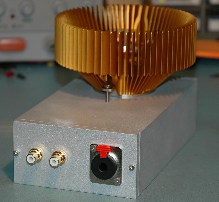
For the rails I’ll probably use a regulated power supply (±17V, each rail approx. 3A).
As you can see, I’ve left out quite a few elements from the Self amp like the built-in options for bridging and paralleling of amplifier boards (not needed here), the unbalanced input (using balanced input from DAC instead), and the DC fault protection mechanism (might still include one, but it doesn’t feel like a big risk here; I will include a MCU that controls a pair output relays to prevent turn-on and turn-off thumps and the like; it would also operate the relay-based volume control mentioned earlier).
Now, for some of the questions:
An overview of the schematic so far has been attached to this post as a PDF:
View attachment 20171020 Schematic.pdf
The DAC I’m using has a balanced analog output, so the amp will be outfitted with a balanced input along these lines:
From left to right, there’s some EMC RF filtering action, followed by non-polarized DC blocking capacitors and an instrumentation amplifier. The DAC that I’m using has an output level of 2Vrms. So, after the instrumentation amplifier, which is configured here with a gain of 2, the ground-referenced signal going into the output stage is 8Vrms max. With my speakers that’s good for about 102dB SPL. As I tend to listen at lower levels, that should be plenty, with room to spare.
I’ll mostly be using surface mount parts; that should also help keep the PCB size within reasonable bounds. I’ve still got a tube with 10 or so LME49990 op amps lying around, but single op amps such as the OPA1611, OPA827 or OPA1641 should also do just fine for U1, U2 and U3. The op amp rails for U1, U2 and U3 are outfitted with a low-pass filter (100Ω thin-film resistor, 22µF polymer tantalum capacitor and a 1µF X7R multilayer ceramic capacitor).
After the balanced input there's an option to hook up a volume control with a unity gain buffer directly behind it (depending on the volume control, R141 might not need to be populated):
I’ve got a relay-based stepped attenuator that could be used here at a later stage. J2 is a 10 position 2.54mm IDC male socket, so that the attenuator board can be connected using a flat ribbon cable. This would let me adjust the system volume outside of the digital domain—somehow I prefer the feel of a solid metal dial over the volume control in Windows.
Finally, we get to the meat of this amplifier in the form of 40 LME49720 dual op amps grouped into 4 arrays:
Each array combines 20 op amp channels followed by 1Ω isolation and current sharing resistors. As Self explains, grouping the op amps like this should make it easier to track down defective ones. 8Vrms into my 6Ω speakers requires 1.3A. I’ve added a few more op amps than strictly necessary so as not to stress them too much. Here, each op amp channel would have to supply 17mA, which is about two-thirds of the typical output current specified in the datasheet.
Each array has its own filtered rails:
Directly next to each op amp is a small 1µF decoupling capacitor.
For stability, at the amplifier output there’s the usual Zobel network and output inductor:
For the rails I’ll probably use a regulated power supply (±17V, each rail approx. 3A).
As you can see, I’ve left out quite a few elements from the Self amp like the built-in options for bridging and paralleling of amplifier boards (not needed here), the unbalanced input (using balanced input from DAC instead), and the DC fault protection mechanism (might still include one, but it doesn’t feel like a big risk here; I will include a MCU that controls a pair output relays to prevent turn-on and turn-off thumps and the like; it would also operate the relay-based volume control mentioned earlier).
Now, for some of the questions:
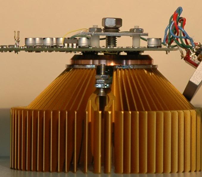
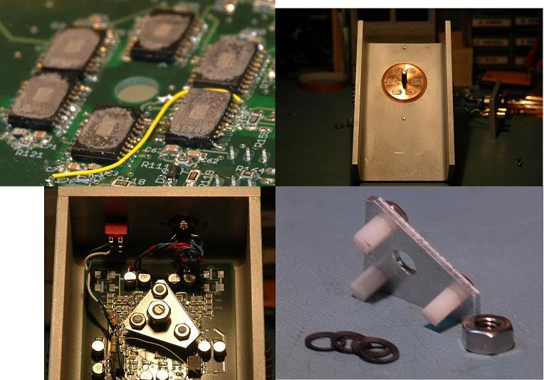
- For sine-wave testing at 8Vrms into 6Ω the amp would probably need some active or passive cooling added. Accounting for the voltage drop in the RCRC filter I reckon that the amp would need to dissipate somewhere in the region of 15-20W per channel. I wouldn’t trust the bare PCB with the op amps on it to be able to shed more than 4W or 5W. But what about when playing music? What would be a realistic estimate when playing, for example, electronic music or jazz at max volume?
- Should I connect the signal ground (XLR pin 1) at the speaker output (or perhaps somewhere else)? Or should I not link it to the amplifier ground at all, and only connect signal ground to the chassis? I’ve found seemingly opposite advice on this from people that all seem like they know what they’re talking about. 🙂
- Where should I ideally connect the grounded leg of R13 (near U3)? Would the connection to ground between R7 and R8 be a good location?
- Would it be worthwhile to nest the output stage in a feedback loop? I noticed that Self did not do this in his design.
Last edited:
JP4 shorts the outputs of two (high current) opamps together. You probably do not want to do this.
The total gain is 2. With 2V Max source and +/-17V rails, you need gain like 5 to justify the excess voltage and heat.
The total gain is 2. With 2V Max source and +/-17V rails, you need gain like 5 to justify the excess voltage and heat.
You have started an interesting project. I have built the Elektor 5532 Poweramp a few years ago. The OPs got really hot, specially in the middle of the PCB. I glued small IC heatsinks on each OP. Of course OPs can handle high temperatures so high temp is not really an issue.
I suggest to consider in your PCB layout some ventilation holes and do not place OPs to close to each other.
Arne
I suggest to consider in your PCB layout some ventilation holes and do not place OPs to close to each other.
Arne
For sure, JP4 can only be used so long as U48 is not populated. 🙂JP4 shorts the outputs of two (high current) opamps together. You probably do not want to do this.
I simmed this configuration yesterday and got an 8Vrms (11.3Vpeak) signal at the output for a 2Vrms signal at IN+ and IN- (the latter of course in anti-phase). So with a gain of 5 it seems like you'd be clipping the signal pretty hard?The total gain is 2. With 2V Max source and +/-17V rails, you need gain like 5 to justify the excess voltage and heat.
I agree that the rails can be sized down though. In the balanced input U3 is loaded the most. Suppose that it draws 20mA max. Then the voltage drop across the 100Ω resistor is 2V. So with a ±15V supply, there's still some 1.7V of headroom until the op amp starts clipping, at least when using a rail-to-rail capable op amp (which the LME49720 is not).
Edit: 10mA max per rail looks to be more accurate, so ±14V could also be okay.
Last edited:
Thanks for sharing your experience with the 5532 amp! Do you still use it? How much of a difference did the heatsinks make?You have started an interesting project. I have built the Elektor 5532 Poweramp a few years ago. The OPs got really hot, specially in the middle of the PCB. I glued small IC heatsinks on each OP. Of course OPs can handle high temperatures so high temp is not really an issue.
That's a good idea. Since I'll have a microcontroller in the amp enclosure I might also add a temperature sensor to each board and maybe power on a fan if the temperature gets out of hand. These SOIC packages don't lend themselves that well to passive cooling.I suggest to consider in your PCB layout some ventilation holes and do not place OPs to close to each other.
Arne
it will be limited by the linear Differential input voltage as well as the rail to rail voltage. With so many op amps 4.7 to 10 ohm output resistors would suffice.
have you listened to a loaded buffer op amp through headphones first to determine which op amp to use before spending $5 apeice on LME part vs $0.15 NE5532?
have you listened to a loaded buffer op amp through headphones first to determine which op amp to use before spending $5 apeice on LME part vs $0.15 NE5532?
In bang-for-the-buck terms there's no competing with the NE5532, but I'm not optimizing for a particular price point here. I'd imagine that it's still the most popular op amp in pro gear for that reason. For this build, however, the enclosure, power supplies and printed circuit boards will probably be bigger expenses. That said, if he LME49720 part would cost US$5 apiece, I'd consider a different IC. Nowadays, it goes for about 1.70 euro in the quantities needed here.Have you listened to a loaded buffer op amp through headphones first to determine which op amp to use before spending $5 apeice on LME part vs $0.15 NE5532?
With parallel discrete output transistors we need to spend time matching them. I wonder if the same is true for parallel opamps? Btw, parallel output devices can never sound as resolving or coherent as a single output device (or opamps). The analogy is the sound of a choir vs a soloist. It's just the limitations of being able to match perfectly.
Intuitively that might seem to be the case, but in practice it's rarely soparallel output devices can never sound as resolving or coherent as a single output device (or opamps). The analogy is the sound of a choir vs a soloist. It's just the limitations of being able to match perfectly.
I’d like to try a headphone amp made with several jrc muse02 op amps, they do some things really well.
I'd recommend higher current, power DSL drivers
parrallel and wrap in a multiloop with good audio input op amp
parrallel and wrap in a multiloop with good audio input op amp
6x TPA6120 dual op amps, rated 400 mA each op amp - parallel pairs biased against each other for Class A push-pull output (a little over 200 mA Class A bias for the headphone amp)
this is sized as a headphone amp so the outputs are cascaded for higher drive V (600 Ohm cans or the insanely low sensitivity AKG K1000)
TPA has exposed Cu power pad meant to be soldered to board for several W dissipation, by soldering "belly up" I contact them to the Cu slug of a pc cooler - running ~ 30 W quiescent total without fan
re arranging the I,V by flat paralleling you could get 2.4A, 15 V peak each channel for ~ 14 Wrms into 8 Ohms Class AB stereo
all up, both channels paralleled as a monoblock the shown components, heatsink should drive down to ~3 Ohms
I designed and built a 16-amp-per-channel stereo 5532 headphone amp inspired by Self's Op-Amplifier. In the end I think it is a stupid idea for a power amp unless 10W is enough power including peaks. This is because the rail voltage is very limited, and that will be the same no matter what small-signal op-amp you choose. The 5532 is good because it is cheap, has very good performance, is well-characterized by Self, and has a low GBW so layout is not so critical, etc. Also, the 5532 generates a bit of heat per IC and this adds up to quite a bit of quiescent dissipation. That would of course be different for other op-amps (e.g. JFET input). For a headphone amp, it actually worked out well because typical drive levels top out around 1Vrms or so, and the rail voltages can be a more reasonable +/-12V. Self really had to push up the rails to the edge of IC reliability to squeeze out as much voltage headroom as possible from the 5532. I learned a good lesson in noise of paralleled amplifiers, and as I increased the number of 5532 amp channels in parallel from 1 to 16 the noise and THD all fell by a good amount, although at the moment can't recall exactly how much. The project is documented on the headphone forum here and was done about 3 years ago IIRC.
Instead of doing this work of folly, build a decent class-A amp of 20W a la FirstWatt, or a quiet single ended amp like the MR7-MKIV. These will be a much better use of your time and money.
Instead of doing this work of folly, build a decent class-A amp of 20W a la FirstWatt, or a quiet single ended amp like the MR7-MKIV. These will be a much better use of your time and money.
Last edited:
Nice amp, I came across it in the other threads. I've a built a few composite amps for my headphones now and they're really fine. I could do something like OPC did with his LPUHP amp, but I chose this approach simply because it puts a smile on my face.😉I'd recommend higher current, power DSL drivers
parrallel and wrap in a multiloop with good audio input op amp
Hey xrk, interesting observation. Is this based on your experience with parallelling the BF862?Btw, parallel output devices can never sound as resolving or coherent as a single output device (or opamps). The analogy is the sound of a choir vs a soloist. It's just the limitations of being able to match perfectly.
With parallel discrete output transistors we need to spend time matching them. I wonder if the same is true for parallel opamps? Btw, parallel output devices can never sound as resolving or coherent as a single output device (or opamps). The analogy is the sound of a choir vs a soloist. It's just the limitations of being able to match perfectly.
This really sounds like BS to me. Got any data to back that up?
Maybe when you are trying to reproduce signals in the 10s or 100s of MHz range... for the audio band the devices themselves are so much faster it should not make a difference.
With parallel discrete output transistors we need to spend time matching them. I wonder if the same is true for parallel opamps? Btw, parallel output devices can never sound as resolving or coherent as a single output device (or opamps). The analogy is the sound of a choir vs a soloist. It's just the limitations of being able to match perfectly.
Or you don't match them and maintain decent emitter resistance. Then the different transistors dither the crossover region.
Applying the same, you of course want output resistors to balance the load. No need to sweat it.
Certainly when opamps are paralleled distortion decreases
NO! That is absolutely NOT correct. It's possible to get reduction in both noise and distortion with many op-amps in parallel. Self has described the noise benefits of parallelization, and you are welcome to check out this post of my measurements, and other posts in that thread:
My LM5532 Headphone Amplifier project - 16 amp stages in parallel per channel (measurements)
Last edited:
- Home
- Amplifiers
- Chip Amps
- Building a massively parallel op amp power amplifier