Also 50mhz clock is a bit tricky to solder and my advice is to put a very thin layer of solder on pcb pads and xo pads and take de surplus with solder wick. This helps in my opinion.
I think the 50mhz xo is the most temp sensitive part from this Dacia.
I think the 50mhz xo is the most temp sensitive part from this Dacia.
Last edited:
Agreeing with Ivan, there is an opportunity for a centralized info and tips collection point that already exists. The first post in a thread remains editable at all times. I'm not sure if I as the first poster have that access alone, or if JP as the originator can also change things. In any event, let me suggest that as a great place/method to publish some basics.
I'd be more than happy to do the collecting and posting, and would encourage builders to include photos with their comments. There is normally a best practices path in most DIY projects and IMHO, lots of unnecessary mistakes could be avoided with some up front information.
As an example - a silkscreen image or schematic that includes all practical test probe locations would be great. I'm sure there are others.
What says the group??
That would be great Bob. Perfect timing because I am about to start testing and those test points would come in handy 🙂
I just fired up my power supply and getting 4.94v. Connected my dac to power supply and no smoke so far.
Any suggestions for next steps?
I just fired up my power supply and getting 4.94v. Connected my dac to power supply and no smoke so far.
Any suggestions for next steps?
Follow the schematic and check if every reg in doing his job, also you can check for dc on output if you want. Afetr that give it a listen and enjoy it.
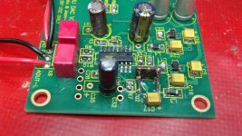
Checking the voltage at the spots on pic L3, L4, L5, L6. That's as far as Iv'e gone.
Attachments

Last edited:
I Did. That was an early shot before the mistake was discovered. I'll post the corrected in that first post group. Doesn't hurt to point it out again though. Thanks.
Thx guys. I am getting 3.3v where you say I should have 0.79v....mmm everything else is correct.
C7...I need to switch around. Could that be it?
C7...I need to switch around. Could that be it?
I removed that photo. Misleading without reading the text. I'll replace it as said in post #168
I switched C7 around but still getting 3.3V
edit...k I see you updated your pic to show 3.3v 🙂
So I should be good to hookup....hope...
edit...k I see you updated your pic to show 3.3v 🙂
So I should be good to hookup....hope...
Last edited:

Observed the following during build when i had some problems with overheated oscillator: if the oscillator is not working on pin 11 of ES9023 you will measure a voltage <1v. When oscillator is working you measure on pin 11 around 3.2-3.3V.
Atupi, do you know which one is pin 11 if the dot on chip is left side?
I am not getting any music from output.
edit...I found a better datasheet....google 🙂
K so I am getting 3.3V on pin 11. Any suggestions?
Last edited:
Any suggestions?
Post some pictures so we can check for any wiring errors.
----Gary
I checked Q2 and noticed that I did not have one of the pads connected. I removed Q2 and put it on its side and then added left over leads to the 2 farthest pads so all 4 are connected. Fired it up and found that L3 is only 0.8V. I checked C19 and I have about 4.5V but C5 only has 1.7V.
I reseated C5 but still get 1.7V.
I reseated C5 but still get 1.7V.
Attachments
Last edited:
I checked Q2 and noticed that I did not have one of the pads connected. I removed Q2 and put it on its side and then added left over leads to the 2 farthest pads so all 4 are connected. Fired it up and found that L3 is only 0.8V. I checked C19 and I have about 4.5V but C5 only has 1.7V.
I reseated C5 but still get 1.7V.
Neville,
What part did you buy for Q2? It doesn't look like the right part.
---Gary
Well, I had it incorrectly positioned. I have all the correct voltages now but still no sound. I suspect I might have fried Q2 because the amount of time I fiddled with it and had an iron to it. I do have 3.3V on pin 11 of ess9023 chip so maybe there is still hope.
Last edited:
All 3 sounding good Atupi ?
Bob, you need C34 + C35 or C34 + C32 and in both cases you can use a SMD cap at the underside of the PCB. Always use C34 ! Try to have a total sum of capacitance larger than 2 µF but not larger than 22 µF.
We did this because MAL128 caps are different in footprint and some of you wanted pads for different caps...Vneg pin is a sensitive one. You will have better results when using larger capacitance than the data sheet value of 1 µF.
Apart from C34 + (C35 or C32) are there any other cap options? I thought I saw somebody asking about C31 vs another cap?
That was probably me. C32 and C31 have a common pad - one on top - one on bottom. I'm still not clear on that arrangement/implementation. Is C31 always installed or is it included in the optional approaches? Though some photos of successful V2 builds with mods in that area have been posted, there still hasn't been a working V3 stock build posted (with photos) that I'm aware of.
Last edited:
- Home
- Source & Line
- Digital Line Level
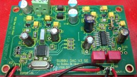
- Build thread - building the Subbu DAC V3 SE