Schematic makes no mention of C31 or .. but I am getting desperate 🙂
Have you got yours working? I have checked WM8804 and ES9023 and both get correct voltages but have no clue what else to test.
If only I could check a signal was coming into 8804 via pin 20, it would be good start 🙂
Have you got yours working? I have checked WM8804 and ES9023 and both get correct voltages but have no clue what else to test.
If only I could check a signal was coming into 8804 via pin 20, it would be good start 🙂
Last edited:
Sadly No. That's why I'm trying to get a step by step build/test procedure established and published. No doubt you and I are not the only builders needing, or will be needing info on a basic operating build. Someone may be close or just hasn't posted yet. We will see what happens when more folks get their parts.
Last edited:
I'm sure we'll know in good time as they respond to questions. I think knowing the important points to probe beyond the basic voltages will be a big boost.
Wonder how Atupi, Asgaard and Gary got theirs working.
Still waiting on the 50Mhz oscillators. They should show up this week.
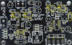
For those needing help, the best thing to do is to post really good pictures where one can see every component clearly. As an example, Neville's pictures would be even better if we could see the face of the Q2 oscillator. Since it's on its side, it's not possible to tell if the orientation is right.
Then take measurements of the voltages on every pin of the WM8804 and ES9023 and compare it to the voltages of known working DACs. There was some discussion where this type of troubleshooting was done in the earlier thread on the original Subbu DAC. Take a look at this thread http://www.diyaudio.com/forums/group-buys/211201-es9023-wm8804-s-pdif-dac-group-buy.html and in particular posts 540 and 552. Those posts show some details on the expected voltages.
---Gary
That's what we needed - thanks so much. Can we assume any changes incorporated in V3 will not effect those readings? If so, could someone point them out.
BTW: The schematic I received had the major voltages only on the sheet. Is there one out there that has them all? There may not be but I thought I'd ask.
BTW: The schematic I received had the major voltages only on the sheet. Is there one out there that has them all? There may not be but I thought I'd ask.
Attachments
Last edited:
That was probably me. C32 and C31 have a common pad - one on top - one on bottom. I'm still not clear on that arrangement/implementation. Is C31 always installed or is it included in the optional approaches? Though some photos of successful V2 builds with mods in that area have been posted, there still hasn't been a working V3 stock build posted (with photos) that I'm aware of.
In the original ES9023 application notes example, there is only one 1 uF cap from NEG (pin 11) to AGND. In V2.6, there is one pad for C32/C35, and one pad for C31/C34 positions. In V3, this same circuit is made up by C31/C34/C32/C35 in parallel. From the BOM notes, I believe it does say C31 or C34 , C32 or C35. So, it is pretty much like V2.6 but with extra pads to "roll your caps".
From experiment and trial perspective, you can try any combination of the above 4 caps as you want, in theory. The only downside might be the excessive desolering from various experiment which can damage the board.
Pchw, you referring to the BOM for 2.6 or 3,0 that has C31 or C34? I dont see it in my v3 BOM? Most of my voltage line up from what I can tell but I need to double check.
Sorry to be so thick headed, but that is clear enough for even me to understand.😱 Thanks. It's looking like there will be several transitions between V2.6 and V3. Hopefully we can eventually sort and post them at the beginning of this thread.
It is V3. The schmatic was from Subbu some time ago.Pchw, you referring to the BOM for 2.6 or 3,0 that has C31 or C34? I dont see it in my v3 BOM? Most of my voltage line up from what I can tell but I need to double check.
From ES9023 pin 11 (NEG), there are 3 caps in parallel to the ground, read as fro m left to right:
C34 (1uF), C31 (1uF), C35/C32 (4.7uF)
FWIW, in V2.6, there is only C31, and it is a film cap (vs a X7R Ceramic in V3) in the "standard BOM". I seem to remember that JP mentioned the reason to change the parts was the Panansonic film cap was too easy to be damaged by heat, but my memory is not something worth to trust 🙂
So, if you are careful with the soldering, maybe that can be another optional parts to try for C31 (ECP-U1C105MA5).
PS: you can send me an email via the forum, I will send you what I got from Subbu.
Thanks,
-fredv-
I checked voltages and I am pretty much spot on except Ess9023 pin 11 & 12 which is 1.7 and WM8804 pin 13 is 0.23V vs 1.02V whish is only big variance.
I resoldered 8804 and some suspect chips but still same result..
Are you suggesting I remove C31 completely and keep C34 ?
I resoldered 8804 and some suspect chips but still same result..
Are you suggesting I remove C31 completely and keep C34 ?
On a whim I removed C31, checked key voltages and connected but still does not fix issue. Henry is correct that his bom shows "c31 or c34" but the bom I have has no mention of it.
Fred, I checked Q2 and pin 1 is not connected to anything, only pin 2 goes to ground.
I'm going to order Q1 and Q2 from Mouser and see if replacing one at time fixes it.
I'm going to order Q1 and Q2 from Mouser and see if replacing one at time fixes it.
Here are my readings. See something - say something. I hope the values in the photo can be adjusted to the correct standard values to serve as a reference document in the thread's first post. Two colors were just for readability - still need some work there.
There is also a printable sheet to record probe values. That also should/will reflect nominal and actual values. The order is from top left - down. then back up in columns. A simple BOM style sheet is coming.
There is also a printable sheet to record probe values. That also should/will reflect nominal and actual values. The order is from top left - down. then back up in columns. A simple BOM style sheet is coming.
Attachments
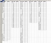
Here are my readings. See something - say something. I hope the values in the photo can be adjusted to the correct standard values to serve as a reference document in the thread's first post. Two colors were just for readability - still need some work there.
There is also a printable sheet to record probe values. That also should/will reflect nominal and actual values. The order is from top left - down. then back up in columns. A simple BOM style sheet is coming.
You've got a problem with the negative charge pump - the voltages at ES9023 pins 9, 10, and 11 are wrong. Check the wiring around components C28 and the various capacitors (C31, C32/C35, C34) hooked up to pin 11. Something is wrong there.
---Gary
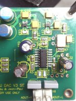
I'd play with it a bit more before reordering. Try resoldering all the connections and see if that helps. Maybe there's a bad solder joint. Or try removing some of the Vneg caps (C32/C35 or C31 or C34) and see if that makes a difference. Perhaps you fried one of the small caps by accident. It would be good if you could narrow the problem further.Can't see any shorts or bridges. Think I should just order replacements for pieces in that area?
---Gary
- Home
- Source & Line
- Digital Line Level
- Build thread - building the Subbu DAC V3 SE