I plan to try it as a balanced to unbalanced converter. My Musician Pegasus r2r dac has both of these outputs, but I want to see if the BTSB can do anything better.Hello everyone, friends. I am surprised how quickly the shipment from Texas Instruments arrived. Yesterday I soldered. It is a new experience for me, working with a hot air station. I hope I didn't screw anything up and BTSB will work. Thank you all for the instructions, advice...

Hi, I'll be soldering my SMT v1.1 board soon. there was a question about negative gain settings
I'm looking for gains close to || -6 / 0 / 6 / xx || or preferably || -6 / -3 / 0 / 6 ||
can you help me out with resistors values (and witch ones) to change?
... thanks 🙂
XRK - just a quick question on this calculation. Reading literally this equation I may use your buffer as a attenuator (by setting R19 higher than R29). But is this a safe in terms of stability and other performance parameters?
I am looking for -9, -6, -3, 0, +3, +6, +6 dB buffer/attenuator/gain stage with BAL/SE/BAL functionality and wondering if such idea is actually a proper one.
Regards,
One of the folks asked if it is feasible to adapt the design from 4 switchable gains to 7. It is if you now use a 6 position dip switch for each positive and negative half into the differential amp and size the input resistor corresponding to all the switches open to the -9dB choice and calculate the remaining ones in parallel with that first resistor to get to the remaining gain choices. As an example, using the feedback resistor of 4K99 an input resistor of about 14K1 results in a gain of about -9dB. If you just want to use the design as it is with different resistor values paralleling the 4K99 input resistance you will onyl realize 4 or 5 practical choices of gain and not the nice spacing you are asking for.
I'm looking for gains close to || -6 / 0 / 6 / xx || or preferably || -6 / -3 / 0 / 6 ||
can you help me out with resistors values (and witch ones) to change?
... thanks 🙂
It’s set up for 0/6/14/20dB. Probably make the range shifted and get rid of 20dB for -6/0/6/14dB. Do this by making Rf half as large Ri. Gain is RF/Ri. With all switches open, it defaults to 4k99 and 4k99 for both RF and Ri. You need to make Ri = 10k so that with all switches open, gain is 0.5x or -6dB. Make the next one 4k99, then 2k49, then 1k24.

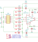
The values look correct. If your goal is an across the board 6 dB reduction it's easier to just change R29, R30 to 2K49. I prefer thin film Susumu resistors in these locations.
You might as well install them to have the option to switch gains. Resistor don’t cost anything compared to the effort and cost of the whole project.
Hi, I wanted to ask a newbie question about this circuit.
In the circuit, I am seeing the differential amplifier feeding the single-ended output in the following circuit:

The newbie question: why is the extra OPA1656 buffer necessary? If we just take the Vout+ from the differential amplifier and GND, won't that be able to drive a single-ended input without any additional buffering?
Please understand, I do not doubt that the circuit behaves very well if I add the buffer. I am only asking, as a circuit designer, not as a BTSB builder, is this buffer necessary whenever I do a balanced-to-single-ended conversion using a differential amplifier? If yes, then where is it necessary,where can it be dropped?
In the circuit, I am seeing the differential amplifier feeding the single-ended output in the following circuit:
The newbie question: why is the extra OPA1656 buffer necessary? If we just take the Vout+ from the differential amplifier and GND, won't that be able to drive a single-ended input without any additional buffering?
Please understand, I do not doubt that the circuit behaves very well if I add the buffer. I am only asking, as a circuit designer, not as a BTSB builder, is this buffer necessary whenever I do a balanced-to-single-ended conversion using a differential amplifier? If yes, then where is it necessary,where can it be dropped?
Last edited:
So if I want to connect only single-ended inputs downstream, I can omit the buffer opamp? Just making sure I understood you right.
The best solution for se output would be a real bal to se converter. If using only one output, buffered or not, is suboptimal.
You might want to Google the Superbal circuit.
Jan
You might want to Google the Superbal circuit.
Jan
I tried Googling "superbal circuit" just now, literally came up with nothing. Google, ever helpful, asked me to try superball circuit. 😁
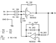
The buffer opamp is needed if differential outputs have DC. Not possible to tell if that is the case as inputs to the FDA (OPA1637) are not shown.
Don't forget that the 'bal' in a bal line stands for impedance balance, not signal balance.
The bal line signals have no ref against gnd, so if you make a se output from one of the bal lines and ground, you re-introduce gnd in the signal chain with a circuit that was not referred to gnd. It may work fine, it may be disaster. Depending.
The superbal circuit takes the bal signal amplitude between the two phases, not using gnd, and constructs the difference signal referred to gnd. That is the best way to avoid ground junk and also maintains the bal circuit because it loads each bal signal with the same impedance, maintaining the bal condition for best hum, common mode and noise supression. The circuit in #451 doesn't do all this, because it does not load the bal signals with equal impedances (even when the resistor values are the same - the impedances seen from the bal outputs are not).
Jan
Last edited:
Ah, understood. And I've seen that two-opamp circuit in books too, I think in Self's Small Signal Circuit Design book too. Thanks for the explanation.
Now to figure out if I can risk dropping the buffer in my case, or if I need to add it.
What would you feel is needed if I use a purpose-built line receiver chip like the THAT 1206 or the INA 134? Will those too need this block downstream?
Now to figure out if I can risk dropping the buffer in my case, or if I need to add it.
What would you feel is needed if I use a purpose-built line receiver chip like the THAT 1206 or the INA 134? Will those too need this block downstream?
- Home
- Group Buys
- BTSB Buffer - SE/Bal to SE/Bal Buffer GB