up until the unity-loop-gain frequency (i.e., the frequency at which the loop came is equal to 1), beyond which it gets more complicated.
... because then there is substantial forward transmission through the FB network?
Jan
... because then there is substantial forward transmission through the FB network?
Jan
Yes, amongst other things. The simplified model assumes signals travel in one direction only i.e. from the input of the amplifier through its various stages to the output, and in the feedback network from the output back to the input. At higher frequencies this is no longer true. Hence the requirement for a Tian or Middlebrook probe for properly measuring loop gain.
LTP or not, bringing the LTP inside the loop (only possible in an inverting configuration) and inverting mode, here a comparison of the two. Would it not be worthwhile to use inverting and an 'extra' line receiver?
Attachments
Last edited:
FdW,
one half of the LTP is not inside the feedback loop in both the inverting and non-inverting arrangements.
In the non-inverting the +IN input is connected via the source to audio ground, whereas for the inverting the +IN input is connected directly to audio ground.
In both arrangements the -IN input is inside the feedback loop.
Is it fair to say one includes the whole LTP inside the feedback loop? and say the other does not?
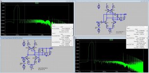
The main point to make is/was that the same components used, one in inverting and the other in non inverting mode, delivers a 30dB difference in THD (yes I know in simulation). This is shown here.
The inverting amplifier shows all transistors inside the loop.
The non-inverting amplifier shows (at the least) Q3 and Q4 outside the loop.
These points where earlier (in this thread) brought to attention.
The inverting amplifier shows all transistors inside the loop.
The non-inverting amplifier shows (at the least) Q3 and Q4 outside the loop.
These points where earlier (in this thread) brought to attention.
The -IN node is inside the feedback loop of BOTH arrangements.The main point to make is/was that the same components used, one in inverting and the other in non inverting mode, delivers a 30dB difference in THD (yes I know in simulation). This is shown here.
The inverting amplifier shows all transistors inside the loop.
The non-inverting amplifier shows (at the least) Q3 and Q4 outside the loop.
These points where earlier (in this thread) brought to attention.
As far as I can analyse (I admit to not being an amplifier expert) the +IN node is not inside the feedback loop in BOTH arrangements.
LTP or not, bringing the LTP inside the loop (only possible in an inverting configuration) and inverting mode, here a comparison of the two. Would it not be worthwhile to use inverting and an 'extra' line receiver?
The first spectra looks a bit strange, to me it looks like the spectrum of a small narrow discontinuity superimposed on the second spectra possibly a simulator artifact. BTW I don't like the SPICE Fourier tool I prefer to export data to a general full complex math tool for analysis. Our inhouse simulator has this built in.
This is an important and in my opinion, under appreciated point. Using a distorting element (ltp common base stage) as the negative feedback summing element is suboptimal in every respect for distortion performance. But that is precisely the configuration (ie non ininverting) that most LTP input stage amps end up with.
The idea of this being an issue only under the condition of large common mode voltages is simply misleading. The issue lies at the heart of the circuit itself.
If you can afford the inconvenience, the inverting mode offers substantially better theoretical (a perfect summing point) , simulated and ultimately, measured performance.
Last edited:
For the inverting amp it is simple, anything between the feedback-summing-point (ideally there will be zero volts) and the output node (marked out) in in the loop, only the input resistor R9 (and the source impedance) is not 'in' the loop. Any distortion in this resistor will show up at the output.
For the non-inverting amplifier it is simple too, Q3 and Q4 are partly in and out of the loop, the most notably (but others may differ and/or add to this) the base-input-current of these transistors can not be corrected inside the loop, the LTP (partly) depends on canceling any effects of this by using totally equal transistors and loading (as discussed earlier in the thread) the distortions of Q3 and Q4 are canceled if they are exactly equal and if the loading (input and output) of these transistors is exactly equal.
IMHO this is a clear case for inverting mode.
The first spectra looks a bit strange, to me it looks like the spectrum of a small narrow discontinuity superimposed on the second spectra possibly a simulator artifact. BTW I don't like the SPICE Fourier tool I prefer to export data to a general full complex math tool for analysis. Our inhouse simulator has this built in.
Who cares, and why then not run it on your 'in-house' simulator. This is all besides the point, the point is not about simulating, the point is INVERTING AMPS HAVE LESS OUTSIDE THE LOOP! and thus (in theory [and probably praxis]) can perform with less distortion. But feel free to run it through the 'in-house' simulator and show us 'better' results 😕
Last edited:
This is an important and in my opinion, under appreciated point. Using a distorting element (ltp common base stage) as the negative feedback summing element is suboptimal in every respect for distortion performance. But that is precisely the configuration (ie non ininverting) that most LTP input stage amps end up with.
The idea of this being an issue only under the condition of large common mode voltages is simply misleading. The issue lies at the heart of the circuit itself.
If you can afford the inconvenience, the inverting mode offers substantially better theoretical (a perfect summing point) , simulated and ultimately, measured performance.

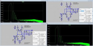
Same simulations with a bit more precision added 🙂
.options numdgt = 7
.options method = gear
.options plotwinsize = 0
Also added a copy for the 'in-house' simulator 🙂
.options numdgt = 7
.options method = gear
.options plotwinsize = 0
Also added a copy for the 'in-house' simulator 🙂
Attachments
May-be you don't use the same protocol ?we have some major difference in our measurements of Damirs 200W CFA. I have measured this slew rate:
I was learned to use this protocol:
1- To remove any low pass input filter.
2- To feed the amp with a square wave signal with a slew rate >10 time faster than the expected result.
3- To feed the amp with a signal much larger than the one that saturate the amp.
4- To take your measurements before the output coil.
5- To measure the slew time of the output signal between +80% and -80% of its peak values. Both ascending and descending.
That is indeed a discourteous and snide remark.
It was just a simple question.
Nonsense. Examples, please.Anyone who looks at what was new in your 6th edition will see that much of that new material was inspired by and along the same lines as, issues that I brought up my first edition - and without proper attribution.
This is an exceptionally egregious statement because it is obvious to every one that your book leans rather heavily on mine, with minimal attribution.
As I have felt obliged to point out before, your book contains hundreds of references, of which just five are to my work. Do you really think that's right?
Examples, please.I believe that there are a number of occasions where you made measurements and speculated wrongly about what was going on.
Please also bear in mind that almost 35 years ago I built and MEASURED a MOSFET power amplifier with error correction and reported distortion levels less than 0.001% at 20kHz up to full power. I'm not sure that, to this day, you have achieved that level of performance in any of your designs. You might want to review that paper; it is on my web site.
That's certainly a long time ago. My last amplifier design for production was in late 2016.
Your point earlier about there being little or no CM in the input stage is not relevant to the issue I have pointed out about your sharing of current source bias lines introducing distorted feedback into the tail current source. Regardless of your motivation for sharing that bias line, be it saving a few pennies or trying to look clever, it is a dumb idea.
At least I was polite about it. And you haven't addressed the point that CM distortion is only detectable with very low closed-loop gains (eg 2x) that put a big CM signal on the input pair.
Last edited:
I thought you had built the SE version?
yes --- that was an SE ips number. Other than a buffer on other input,
SIM shows no significant difference but will get to that later.
THx-RNMarsh
Dear Richard,
we have some major difference in our measurements of Damirs 200W CFA. I have measured this slew rate:
(scope screen shot here: 200W MOSFET CFA amp)
- 10kHz square rising edge (slew: 70V in 250ns ~ 280V/µs)
- 10kHz square falling edge (slew: 70V in 375ns ~ 200V/µs)
200W into any load and frequency also different: 200W MOSFET CFA amp
My measurements differ from yours significant. It looks like your test sample has a different - more aggressive - compensation or is different in using other components?
IMHO: the amplifier has very good values - I do not want to make Damir's amplifier look bad in any way! I just want to know why we measure such different values...
We could continue this discussion in Damir's thread or start a new one.
BR, Toni
Its in your construction wiring layout and grounding system. Not the circuitry. Both internally and/or the testing setup.
SR is without the input RC filter.
You are comparing THD+N to my THD. (But I have both numbers and you are are still a bit higher, over-all. So, its your wiring/grounding needs improving).
THx-RNMarsh
Last edited:
The inverting input .... the input R is in series with the source output R... The source output may include a build-out resistor. depending on the source topology --- affecting gain. And, it's Zo may not be constant with frequency.... OPS Zo of source will depend on topology -- interconnect cable Ls and amount of neg feedback or none in preamp/source etc.
Again, a X1 buffer might be needed on IPS of receiving end/PA for a better defined source Z to the ips of inverting amp. .
So to avoid variations from listener to listener's SYSTEM, I have to avoid the inverted config. Also, the signal polarity inversion is not always a good thing in audio.
THx-RNMarsh
Last edited:
Some people claim, absolute polarity can be heard, e.g. on certain attacks. Can you support that from experience?Also, the signal polarity inversion is not always a good thing in audio.
The inverting input .... the input R is in series with the source output R... The source output may include a build-out resistor. depending on the source topology --- affecting gain. And, it's Zo may not be constant with frequency.... OPS Zo of source will depend on topology -- interconnect cable Ls and amount of neg feedback or none in preamp/source etc.
Yes, I know, most here know, and was discussed, a buffer will solve this and leaves you with a phase correct amplifier having (except for that one resistor) everything inside the loop.
Again, a X1 buffer might be needed on IPS of receiving end/PA for a better defined source Z to the ips of inverting amp. .
Yes.
So to avoid variations from listener to listener's SYSTEM, I have to avoid the inverted config. Also, the signal polarity inversion is not always a good thing in audio.
The signal polarity problem can be solved by reversion the LS connection polarity.
Why talking about trivialities, and not about input-current-distortion and it's solutions (like not using an LTP or using an inverting amplifier or ... some other solution).
- Home
- Amplifiers
- Solid State
- Bob Cordell's Power amplifier book