E Stuart why has no one built your circuits? I have admired what seems to be lots of hard and good work on your part, but it seems as if no one wants to take the task of layout and assembly, then test...Complex but DOable from my perspective...
"why has no one built your circuits?" Good question, but I don't know the answer. Probably it's a little too complex and/or everyone is waiting for real life result from this amp when built by myself.
Meanwhile, I've purchased almost all components for this amp, but my distortion analyzer has to be finished first.
Cheers, E.
[snip}
Measuring the emitter resistor Re does not depend on temperature, you monitor and adjust the current, which is the ULTIMATE goal of this whole thing. Who cares about temperature?
[snip]
Exactly!
Cheers, E.
Edmond, just so you don't feel totally out in the cold 🙂, I played around with your ideas in LTspice at one stage, and got some very impressive results - it should be capable of doing excellently ... one of the many things sitting in the To Do bin ... 🙄"why has no one built your circuits?" Good question, but I don't know the answer. Probably it's a little too complex and/or everyone is waiting for real life result from this amp when built by myself.
E Stuart why has no one built your circuits? I have admired what seems to be lots of hard and good work on your part, but it seems as if no one wants to take the task of layout and assembly, then test...Complex but DOable from my perspective...
I know somebody that attempted to build it, and it was a total failure. The circuit latches up when the output is approaching the rails and the signal is fast enough (1KHz is good, 10k already triggers the issue). Something the author also got in simulation, and tried to patch with a second order filter at the input. Not good enough in practice.
Until it latches, the circuit has very low distortions indeed.
Originally Posted by jan.didden
The voltage across an Re is NOT an AC signal you can just low-pass!
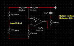
I've been thinking about this since you replied to my http://www.diyaudio.com/forums/solid-state/277005-oliver-offset-optimiser.html circuit idea etc earlier. How about this instead with that ?
Originally Posted by jacco vermeulen
I have a design somewhere with an individual driver per output device, which enables to bias each power device separately without loading the Vas.
I've often thought that individual drivers per output device might be a good idea. Be nice to see your circuit 🙂
Attachments
Hate to splash some cold water, all these are to protect the thermal run away. BUT if one of the circuit that control the current goes south, it's can be smoke city!!!😀😛
I've been thinking about this since you replied to my http://www.diyaudio.com/forums/solid-state/277005-oliver-offset-optimiser.html circuit idea etc earlier. How about this instead with that ?
I think the output of that one will be a lowpassed sum of the drop across both resistors (the opamp would need to operate at or above the output's supply voltage). But, when the amp is delivering output current, the sum voltage will rise, even if bias is correct, the result being a filtered full-wave rectified version of the output current. Fine for class A, not fine for class AB.
"why has no one built your circuits?" Good question, but I don't know the answer. Probably it's a little too complex and/or everyone is waiting for real life result from this amp when built by myself.
Cheers, E.
A little complex? This is complex big time!!! For truly controlling the current and balance the current for different parallel pairs, you have to control current for each individual transistor. So if you have 5 pairs of output transistors, you need 10 individual servo circuits!!! If you control one, you cannot guaranty the others are not going to hog current.
You likely have to go 4 layers pcb to keep the size down, then you still have programming to do.
And the most important of it all, power amps have been very reliable. You want to be safe and lower distortion? go with more pairs of transistors. The more pairs you have, the more pairs to share the current. The more pairs, the lower the distortion that has been explained by Self's book.
With all the complexity, I can easily add 3 more pairs and make mine 8 output pairs to lower distortion and,.....don't tell me I will still have hogging problem if I just match beta of those transistors. The more I read and think about this, the more it make sense for me to sent out the new layout of OPS pcb with 8 pairs of transistors. Just let me power up the 5 stages first to see the result. The 8 pairs is going to be close to half the distortion of a 5 stages if all else are the same.
Well said!But, when the amp is delivering output current, the sum voltage will rise, even if bias is correct, the result being a filtered full-wave rectified version of the output current. Fine for class A, not fine for class AB.
I asked a couple of questions in [url]www.diyaudio.com/forums/solid-state/171159-bob-cordells-power-amplifier-book-613.html#post4393625[/URL] that HAVE to be answered regardless of whether you use analogue or digital means to control bias.
The success of a bias scheme is measured by how successfully ANY scheme answers ALL the questions. 😱
IMHO, the 'perfect' bias scheme is sorta shown by a pic in one of Jan Didden's links to his Linear Audio books. As a beach bum, I'm unlikely to buy one of his books but this article was very tempting.
Dunno which one cos its a zillion pages back and obscured by all da useless BS about class 😱
_____________
IMHO, the chapters on Thermal Design in both Cordell & Self are the most valuable in both books .. even though they disagree with each other and I disagree with both.
All the other stuff can be found elsewhere (with due respect to both Gurus Cordell & Self 🙂 ) if not in quite as clear and accessible form.
But the respective tools they present allow you to 'design' (???) your own thermal behaviour.
I don't think the ultimate chapter has been written about this subject and I thank both Gurus for their attempts.
The reason I disagree with both is I don't think they address my questions in http://www.diyaudio.com/forums/solid-state/171159-bob-cordells-power-amplifier-book-613.html#post4393625
And those chapters have sorta led to these last zillion or so pages which at least bring out loadsa opinion & hopefully 'real life' experience on the subject.
______________________
For the new DIY ampbuilder, I advise discounting heavily the opinions of the "my devices are hand-selected by Virgins after washing in liquid Unobtainium and the ONE amp I've built is OK" brigade .. that is if the release of Holy Smoke might be embarrassing to you
I've also conducted numerous DBLTs that prove liquid BS is a suitable substitute for liquid Unobtainium and much more freely available. eg liquid BS flows in inexhaustable quantities in these forums. 😎
______________________
Lastly, at the risk of even more Heresy 😱, all these evils pre-suppose the ops is a voltage follower.
But what if you current drive it? While Guru Self recovers from his apopletic state, here are a few probable 'features'
- THD introduced by the ops is now MUCH lower order eg simple change of slope due to mismatched hfe instead of yucky turn on/off, xover, Oliver-or-not bla bla
- you'll have LOADS more loop gain to reduce these lower order harmonics
- bias becomes MUCH less critical eg a 2:1 change is unlikely to affect your 1pp zillion THD20k
A simple way to achieve this is to adopt Pure Cherry Compensation.
Guru Self will tell us he is unable to make it work but that doesn't stop the rest of us from doing so 🙄
Last edited:
Tell me what is the main cause of current hogging? In a multi transistors EF in parallel, what make one device pull more current than the others?For the new DIY ampbuilder, I advise discounting heavily the opinions of the "my devices are hand-selected by Virgins after washing in liquid Unobtainium and the ONE amp I've built is OK" brigade .. that is if the release of Holy Smoke might be embarrassing to you
Last edited:
It's already been explained at length by various people in the last zillion or so posts.Tell me what is the main cause of current hogging? In a multi transistors EF in parallel, what make one device pull more current than the others?
It comes from the temperature dependence of Vbe vs current. BUT there are a host of inter-related factors .. to name a few, hfe & Vbe matching, Re, Rb, Thermal Design, SOA, actual power dissipation with load & signal etc.
My take from the zillion posts is that devices are both faster and much more robust today and heatsinks usually bigger than the early 70's. Also, DIYs like you today, think nothing of using zillion o/p devices for relatively small amps. In this case, the lesser dissipation/device might more than compensate for any possible 'hogging' depending on matching, Re, Thermal, SOA bla bla.
When there are so many factors, the important data points are 'real life'. eg
RNMarsh reduced Re on a big 2x200W 8R amp and found improved THD .. the price being having to replace all the outputs every 12mths or so. Details of the Thermal Design, output stage, bias currents bla bla would be useful as something that's probably ju..uust on the edge.
Self tells us he uses 0R1 Re on his zillion device big amps without problems and they have made zillions. His EXACT Thermal Design, bias, bla bla is of interest ... provided his info is reliable.
Rotel made a couple of 2x200W 8R amps circa 1980 that used only 2 pairs of o/ps on relatively small H/Ss with minimal protection (current sense opening a relay) It regularly survived the usual screwdriver SC test. Rotel are not known for making unreliable amps.
My guess is Re 0R47 and the robust o/p devices used.
British designers of that period would not have done anything so crude .. cos they couldn't get the good robust devices. 😡
What you look at and/or agonise over depends on whether you are making one or many, and if failure would embarrass you.
So don't expect a 'single answer' to your question unless its a VERY conservative one.
It comes from the temperature dependence of Vbe vs current. BUT there are a host of inter-related factors .. to name a few, hfe & Vbe matching, Re, Rb, Thermal Design, SOA, actual power dissipation with load & signal etc.
1) Vbe with temperature is about -2mV, device of the same number eg. MJW1302 are going to be closely matched as long as you use the same parts.
2) Vbe can be matched easily to 1 or 2 mV by testing and grouping. Far as my understanding, Vbe behaves the same whether it's DC or AC signal.
3) hfe needs to be matched, That that can be matched to within 2%. Far as my understanding, hfe behaves the same whether it's DC or AC as long as you are not pushing fT.
4) Re is resistor matching, you can buy 1%.
5) Rb is important as base current cause voltage drop....again this goes back to hfe.
6) Of cause you have to do SOA and thermal design whether you match transistors or not.
So tell me what is wrong of picking transistors by matching hfe and Vbe? I did matching over 50 of each NPN and PNP in less than 2 hours. What is so wrong of matching transistor where all the discussions so far involve much more complex uP servos, programming and all?
For the servo current control, you are going to have to do servo on individual transistor, you have to make the board larger, likely 4 layers, more parts to buy and more time to program.
What's wrong with instead doing the complicate work, put in more output pairs so you don't push the SOA and power limit? More pairs guaranty you have lower distortion. It is well documented that the higher the load resistance, the lower the crossover distortion. Using more pairs will make the apparent load resistance for each pair higher. This is well documented in both Cordell and Self's book. eg. If you drive a 4 ohm speaker, if you use 4 pairs, each pair only see the apparent load impedance of 16ohm as the 4 ohm is split between 4 pairs.
Maybe Mr. Cordell can jump in if I miss anything. That if you match Vbe and hfe, then with good heatsink design, you should not have current hogging problem no matter at idle and with larger signal.
Last edited:
"why has no one built your circuits?" Good question, but I don't know the answer. Probably it's a little too complex and/or everyone is waiting for real life result from this amp when built by myself.
Meanwhile, I've purchased almost all components for this amp, but my distortion analyzer has to be finished first.
Cheers, E.
I'll test it for you, if you like.
THx-RNMarsh
I'll test it for you, if you like.
THx-RNMarsh
There were some extensive simulations with Edmond's AB2 circuit in "Class i and siblings" thread.
Damir
The 26mVre from the Oliver condition ONLY applies for one fixed temperature. Approximately 300KI think monitor ONLY the current of the Re is much better way to do it because you totally eliminate the temperature term in the whole equation. .....................
Measuring the emitter resistor Re does not depend on temperature, .............
If the temperature of the junction varies from that fixed value, then the Vre also changes in direct proportion to the absolute temperature change
300K ~ 27°C, 26mVre
330K ~ 57°C, 28.6mVre
360K ~ 87°C, 31.2mVre
A hot amplifier requires a different Oliver voltage condition from a cold amplifier.
One can choose to ignore changes in output stage temperature, but it should be better to take account of temperature.
I wonder if the slight over-bias condition helps with maintaining a closer approximation to the Oliver condition, since that would suit the working temperature range of typical warm amplifiers?
Last edited:
Lastly, at the risk of even more Heresy...
But what if you current drive it?...
A simple way to achieve this is to adopt Pure Cherry Compensation...
Hi Richard
This looks to me a little like the interminable debate(s) about whether to conceptualize a transistor as "current driven" and focus on hFE or "potential driven" and look at the Vbe and Ic relation.
The maths must work out the same either way.
Spice uses a Modified Nodal analysis so it's transadmittance that is actually calculated, for any connection.
I see Cherry aka Output Inclusive Compensation as just a different feedback loop connection.
But I have to admit I have several times read Cherry's JAES papers on this subject and still don't really have a "feel" for his discussion of Vbe non-linearity versus hFE nonlinearity.
Sometimes he seems to miss aspects, not sure if he just wants to sweep them under the carpet to avoid discussion.
Can you expand on your point?
Best wishes
David
Last edited:
The 26mVre from the Oliver condition ONLY applies for one fixed temperature. Approximately 300K
If the temperature of the junction varies from that fixed value, then the Vre also changes in direct proportion to the absolute temperature change
300K ~ 27°C, 26mVre
330K ~ 57°C, 28.6mVre
360K ~ 87°C, 31.2mVre
A hot amplifier requires a different Oliver voltage condition from a cold amplifier.
One can choose to ignore changes in output stage temperature, but it should be better to take account of temperature.
I wonder if the slight over-bias condition helps with maintaining a closer approximation to the Oliver condition, since that would suit the working temperature range of typical warm amplifiers?
Alan, this is a very good point, being that kT/q is PTAT. However, the differences in desired Vre may not be big enough to really worry about too much in the big picture. Going from 27C to 87C changes Vre by only 5mV. I think we would all cheer if we could keep Vre within that tolerance over all real-world operating conditions and realities.
But let us keep a couple of things in mind. First, going under-bias is worse than going over-bias. Secondly, at idle, the junction temperature is always going to be above room temperature, perhaps 35-40C, so the nominal design may want to be a tad higher than 26mV.
Cheers,
Bob
cos they couldn't get the good robust devices.
Could not, or would not ?
- Home
- Amplifiers
- Solid State
- Bob Cordell's Power amplifier book