I've worked out how this could be done, but obviously it has potential commercial implications. So if someone with such connections is interested in persuing this, PM me 😉
So what about being a sport and help review one of your own designs, so much for helping the DIY community.
I've worked out how this could be done, but obviously it has potential commercial implications. So if someone with such connections is interested in persuing this, PM me 😉
Hi Zero D,
That's great. New ideas are always welcome, and we all learn from them, even if they don't turn out as expected. Over the years most of the folks on this forum have come up with some new solutions to problems. Unfortunately, the reality is that virtually none of these ideas and techniques end up having any monetary value insofar as things like royalties. Unless it is monumental, the cost and hassle of protecting such an idea to reap some income from it is just not worth it. Life is too short.
So I encourage you to post your idea here for all to see and learn from. If you do, I'll promise to respond with a post here letting you know what I think of it with constructive feedback.
Cheers,
Bob
Hi Doug,
My mistake, your book is where I think I first saw the term. I didn't realize you did not like the term. Any idea who came up with the term?
Hello Bob
I've no idea. I can only say it was a common term in 1993. A trawl back through Electronics World from that year would probably turn it up.
Thanks , Bob.
The "collapse" simulations are with a 1uf bypass.
"testpig" (below pix) shows the standard spreader.
"A" is the Locanthi configuration.
"B" options are for an EF2 IRFP OPS.
I was thinking about a project associated with your book.
You are most famous for your old "HEC" OPS.
(attached PDF below) is what one member "morphed it" into.
I have the original simulation based on your paper and (a simulation)
of this one.
The attached one is very promising. Our member LKA has built it , as well.
It brings many of my IPS's solidly into the sub PPM realm !!
OS
Hi OS,
Thanks for this info. Looks like the total Vbe multiplier resistance is about 4.8k with a little less than 1mA flowing through it. If you made that 1uF spreader bypass much larger (at little expense) might you expect any improvement in performance right after the amp comes out of a low-frequency clipping interval (in regard to the SQ of the higher frequencies passing through during the subsequent brief under-bias of the output stage)?
Conversely, do you see any downside to using such a much larger capacitor to mitigate what admittedly is a shortcoming that may have no audible effect?
I like that implementation of HEC using what is effectively a Diamond Buffer Quad. It is a nice way to get the necessary spread for the HEC circuit to work.
Cheers,
Bob
"Pick your poison" 😀 Small cap , faster dynamic feedback. Large cap ,
reduces the collapse.
The OEM's have opted for the former in "hi-end" spreaders. t-trak spreader =
470nF - 1uf , 2 device spreader = 1-2.2uf.
The only 22uF + bypass I've seen in my 1K service e-manual
collection is on "low-fi" simple 40W receivers and such (BJT EF2).
OS
reduces the collapse.
The OEM's have opted for the former in "hi-end" spreaders. t-trak spreader =
470nF - 1uf , 2 device spreader = 1-2.2uf.
The only 22uF + bypass I've seen in my 1K service e-manual
collection is on "low-fi" simple 40W receivers and such (BJT EF2).
OS
Gm Doubling...a fiction?
I went searching for the history of the term, and came upon an interesting paper by Marshall Leach:
http://users.ece.gatech.edu/mleach/papers/classab.pdf
Yes, he shows wiggles in the transition region open loop gain of the output stage, but he also shows that the gm never doubles for any practical choices. He also puts forth a theory for where this "gm doubling" notion might have arisen.
Yes, I'm familiar with that paper. I believe that the gm doubling term comes from the fact that, in the limit, with ideal transistors that are voltage-fed, the gm will be twice as much at crossover (no net output current) as at high plus or minus output current extremes. This is because, conceptually, both transistors are contributing transconductance through RE in the class-A region and only one transistor is contributing transconductance through RE in the outer class B region.
In practice, this generally does not happen to nearly this extent. I'm guessing you can maybe get to gm * 1.5 in reality if you try.
Cheers,
Bob
OPS Temp Monitor & Control
Yeah, like one of my previous ideas, eg the Loop Gain Enhancer thingy ! It worked OK, & with kind help from HarryDymond it was made even better. It turned out it was similar to one of Bonsai's ideas !
Yeah, life can be a bitch sometimes 😀
You've twisted my arm 😉
Well i havn't got a circuit, just the general idea. This consists of monitoring the OPS devices with an IfraRed detector element. For eg, as fitted to sucurity lights & burgler alarm sensors etc. The detected voltage would then feed the bias control etc etc.
Originally Posted by Bob Cordell
Hi Zero D,
That's great. New ideas are always welcome, and we all learn from them, even if they don't turn out as expected.
Yeah, like one of my previous ideas, eg the Loop Gain Enhancer thingy ! It worked OK, & with kind help from HarryDymond it was made even better. It turned out it was similar to one of Bonsai's ideas !
Unfortunately, the reality is that virtually none of these ideas and techniques end up having any monetary value insofar as things like royalties. Unless it is monumental, the cost and hassle of protecting such an idea to reap some income from it is just not worth it. Life is too short.
Yeah, life can be a bitch sometimes 😀
So I encourage you to post your idea here for all to see and learn from. If you do, I'll promise to respond with a post here letting you know what I think of it with constructive feedback.
You've twisted my arm 😉
Well i havn't got a circuit, just the general idea. This consists of monitoring the OPS devices with an IfraRed detector element. For eg, as fitted to sucurity lights & burgler alarm sensors etc. The detected voltage would then feed the bias control etc etc.
I went searching for the history of the term, and came upon an interesting paper by Marshall Leach:
http://users.ece.gatech.edu/mleach/papers/classab.pdf
Yes, he shows wiggles in the transition region open loop gain of the output stage, but he also shows that the gm never doubles for any practical choices. He also puts forth a theory for where this "gm doubling" notion might have arisen.
I have only had a quick look at the paper but this may be the old confusion about the term Class-AB. Looks like he's using it to mean optimally biased Class-B, which naturally has no doubling. Crank up the bias to get into real AB, with a substantial area of Class-A operation, and gm-doubling (or "gain-deficit-halving") appears. Easily simulated, eg Figure 9.10 in APAD6.
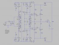
Here is a gain of one Output stage with very good performance.
Total Harmonic Distortion: 0.006294% @ 20KHz 60V/pp
I use the folded cascode to make a very direct feedback injection around the output devices.
Off-course it's also possible to insert a VBE and an EF3 OPS.
The cascoded jfets makes it possible to have high input impedance.
Total Harmonic Distortion: 0.006294% @ 20KHz 60V/pp
I use the folded cascode to make a very direct feedback injection around the output devices.
Off-course it's also possible to insert a VBE and an EF3 OPS.
The cascoded jfets makes it possible to have high input impedance.
Attachments
I have only had a quick look at the paper but this may be the old confusion about the term Class-AB. Looks like he's using it to mean optimally biased Class-B, which naturally has no doubling. Crank up the bias to get into real AB, with a substantial area of Class-A operation, and gm-doubling (or "gain-deficit-halving") appears. Easily simulated, eg Figure 9.10 in APAD6.
Hi Doug,
I think Marshall is using the term class AB to describe what you refer to as optimally-biased class B, as I do. Oh, those semantics again!
On the forum here we constantly talk about the class A region of such an output stage, often referring to the peak amount of output current at which the stage enters class B where only one output device is on. So, with a "class A region", how could one not call it a class AB output stage?
Consider the output stage beast we are talking about when it has 4 output pairs, each with RE=0.22 and bias of 118mA, for a total bias of 472mA (satisfying the Oliver criteria). It will be in the "class A" region up to an output current of 944mA. This corresponds to 3.6 watts into 8 ohms. That is quite a bit of class A power to be referring to the beast as class B.
Into 90dB SPL 1w loudspeakers, it will produce 95dB SPL at 1 meter - quite loud.
Sorry to beat this poor dead and bleeding horse again.
Anyway, to each his own 🙂.
Cheers,
Bob
Hi Bob, and others, may i ask a newbie question, how do you draw the line between a classB and an AB in terms of output stage bias? can you cite figures for comparison?
Just say it, he make up all the terms to be special. I don't know what other way to put it. Blameless, Class B, XD.......Hi Doug,
I think Marshall is using the term class AB to describe what you refer to as optimally-biased class B, as I do. Oh, those semantics again!
On the forum here we constantly talk about the class A region of such an output stage, often referring to the peak amount of output current at which the stage enters class B where only one output device is on. So, with a "class A region", how could one not call it a class AB output stage?
Consider the output stage beast we are talking about when it has 4 output pairs, each with RE=0.22 and bias of 118mA, for a total bias of 472mA (satisfying the Oliver criteria). It will be in the "class A" region up to an output current of 944mA. This corresponds to 3.6 watts into 8 ohms. That is quite a bit of class A power to be referring to the beast as class B.
Into 90dB SPL 1w loudspeakers, it will produce 95dB SPL at 1 meter - quite loud.
Sorry to beat this poor dead and bleeding horse again.
Anyway, to each his own 🙂.
Cheers,
Bob
Just say it, he make up all the terms to be special. I don't know what other way to put it. Blameless, Class B, XD.......
.
Last edited:
Hi Doug,
I think Marshall is using the term class AB to describe what you refer to as optimally-biased class B, as I do. Oh, those semantics again!
[snip]
Anyway, to each his own 🙂.
Cheers,
Bob
This was discussed a few pages back. I suggested there should be a defined cutoff for the size of the class A region, in terms of % of rated output, below which a stage should be called class-B and above which it should be called class-AB. I suggested 3% but there was disagreement about whether this threshold was too high (ie 2.5% class-A region could be considered "significant" in absolute terms for an amplifier with high rated output such as 400 W.)
Would you agree that the term class-AB by itself does not convey sufficient information about the operation of the output stage? After all, according to many here and many text books it could refer to an amplifier whose class-A region is anywhere from >0% to <100% of the rated output power.
How about appending a simple numerical quantifier, which indicates size of the class-A region as a percentage of rated output power? For example, class-A01B for an amplifier with 1% class-A region, class-A20B for one with 20% class-A region, etc?
Hi Bob, and others, may i ask a newbie question, how do you draw the line between a classB and an AB in terms of output stage bias? can you cite figures for comparison?
One cannot draw a bright line between class B and class AB because in reality the cutoff of the transistors is not sudden, as a result of the exponential Ic vs Vbe relationship. It takes a long way (amount of voltage, in relative terms) to get the transistor truly into cutoff, as it is approached somewhat asymptotically. With every 60mV of reduction in Vbe, the collector current will decrease by a factor of 10. A transistor nominally biased at 100mA will still be conducting 1mA when Vbe has decreased a full 120mV. It will still be conducting 1uA when Vbe has decreased yet another 180mV. In theory, it never quite gets there. So the declaration of cutoff for purposes of definition of class B must be rather arbitrary, but reasonable. This is similar to what Harry is saying.
I would say that class B is the case when no intentional extra bias is applied beyond that which prevents significant notch distortion. The Oliver criteria constitutes the deliberate and controlled application of a bias that is greater than that. Perhaps any bias that is substantially less than the Oliver bias would qualify the output stage as being deemed to be class B. Perhaps "substantially less" could be arbitrarily defined as one-half.
Just my $0.02.
The horse is really mangled now 🙂.
Cheers,
Bob
Why not use the terminology of what it used to be..... no need to change it...... Class of Operation is defined by its conduction angle. ??
THx-RNMarsh
THx-RNMarsh
Last edited:
One cannot draw a bright line between class B and class AB because in reality the cutoff of the transistors is not sudden, as a result of the exponential Ic vs Vbe relationship. It takes a long way (amount of voltage, in relative terms) to get the transistor truly into cutoff, as it is approached somewhat asymptotically. With every 60mV of reduction in Vbe, the collector current will decrease by a factor of 10. A transistor nominally biased at 100mA will still be conducting 1mA when Vbe has decreased a full 120mV. It will still be conducting 1uA when Vbe has decreased yet another 180mV. In theory, it never quite gets there. So the declaration of cutoff for purposes of definition of class B must be rather arbitrary, but reasonable. This is similar to what Harry is saying.
I would say that class B is the case when no intentional extra bias is applied beyond that which prevents significant notch distortion. The Oliver criteria constitutes the deliberate and controlled application of a bias that is greater than that. Perhaps any bias that is substantially less than the Oliver bias would qualify the output stage as being deemed to be class B. Perhaps "substantially less" could be arbitrarily defined as one-half.
Just my $0.02.
The horse is really mangled now 🙂.
Cheers,
Bob
thanks Bob...
Why not use the terminology of what it used to be..... no need to change it...... Class of Operation is defined by its conduction angle. ??
THx-RNMarsh
Two issues I have with defining it by conduction angle:
1. If you define class-B as 50% conduction, what exactly does that mean? It has to be 50.0000000000000% to be class-B? What about 50.1%? Is that B or AB? Achieving exactly 50% conduction angle under all operating conditions is both impossible and pointless and it seems odd to relegate an entire class designation to being something that is physically unrealisable.
2. It leaves -AB to cover all conduction angles from >50% to <100%, despite the very wide range of static power dissipation, full-power distortion, and low-power distortion that this range covers. Again, it seems odd to me to have a single term that covers such a wide gamut of operating conditions.
- Home
- Amplifiers
- Solid State
- Bob Cordell's Power amplifier book