Question ----
The two legs of the spreader (sounds obscene) are bypassed.... I usually use a very large value, in the past, no sim.... just thought that the DC voltage across the C (Vbias) charges that cap and will help to maintain the DC bias level at a fixed/constant level.... pro-con to doing this ref. thermals ???
THx-RNMarsh
Last edited:
I wonder whether this mechanism accounts for some audible differences between amps? I mean, beyond the obvious generation of harmonics when clipping?
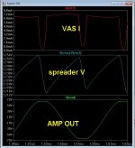
It would be interesting to see these waveform with a low level higher freq signal say 1kHz superimposed?
Jan
There you go , Jan. (below).
Your "audible" question is hard to comment on.
Before clipping you only have that minimal ripple that you see in the blue trace.
During clipping , if you go fully into class B ... that actually makes
the output stage's work easier. BTW , this "effect" is very minor
with my spreader and EF3 , I had builders grossly overload these
circuits to arrive at the final design.
All this with the VAS's impedance and spreader values works very
well with an EF3. The "mechanism" is far worse with a EF2 (or
with a "blameless" VAS).
Curious that anybody is even interested ? Some EE's say ... " just
don't let it clip". 🙄
OS
Attachments
I thought that the Sankens were a problem because there was not enough output transistor base pull-down current to suck out minority carriers fast enough at high frequencies, and that there was no opportunity to increase it by external means. Am I wrong? What is the nominal amount of base turn-off current built into these devices?
Cheers,
Bob
Bob, I really don't know the resistor value of the B-E resistor in the final device. You are correct that it's not accessible. I never noticed an issue with that - then again my amp doesn't get the low THD numbers of your MOSFET amp.
One practical advantage is that with a medium-power driver and the Sankens you can build a compact 3EF output stage for say up to 100W/8ohms equivalent. The pin layout of the N and P are mirror images.
They even used to have a version with Re (0.22) build-in, but that was discontinue after field failures turned up with Re open and the transistor intact...
Jan
Attachments
There you go , Jan. (below).
Your "audible" question is hard to comment on.
Before clipping you only have that minimal ripple that you see in the blue trace.
During clipping , if you go fully into class B ... that actually makes
the output stage's work easier. BTW , this "effect" is very minor
with my spreader and EF3 , I had builders grossly overload these
circuits to arrive at the final design.
All this with the VAS's impedance and spreader values works very
well with an EF3. The "mechanism" is far worse with a EF2 (or
with a "blameless" VAS).
Curious that anybody is even interested ? Some EE's say ... " just
don't let it clip". 🙄
OS
OS, thanks for that, but what I meant was you have say 50 or 100Hz signal, clipping and all the bad things on the spreader voltage. BUT at the same time there is a low level say 100mV 1kHz signal also, riding on the 100Hz. I was curious how the 1kHz would look in this situation - just 'clipped' or something else?
Jan
Question ----
The two legs of the spreader (sounds obscene) are bypassed.... I usually use a very large value, in the past, no sim.... just thought that the DC voltage across the C (Vbias) charges that cap and will help to maintain the DC bias level at a fixed/constant level.... pro-con to doing this ref. thermals ???
THx-RNMarsh
But you still want a certain degree of dynamic response in the spreader.
A large bypass is good for a "amateur" design.
Ideal is a timing close to the output slug's thermal response.
This is nearly impossible to do with the spreader on top of the output
or on the extrusion. Epoxy thermal resistance or the equilibrium of the extrusion are limiting factors.
Only the t-trak or a two device spreader can bypass this.
OS
OS, thanks for that, but what I meant was you have say 50 or 100Hz signal, clipping and all the bad things on the spreader voltage. BUT at the same time there is a low level say 100mV 1kHz signal also, riding on the 100Hz. I was curious how the 1kHz would look in this situation - just 'clipped' or something else?
Jan
Oh , that's all (below 1-2).
The higher freq. waveform will clip until full saturation right at the ""cutoff
point". My vas actually cuts off (clamps) within the baxandall at this point.
It also goes high Z .... reacts differently than a current sourced VAS
in regards to the spreader voltage.
This "generation" amp (below 3) has been described as "tube-like" when
builders/testers have actually clipped it.
OS
Attachments


They even used to have a version with Re (0.22) build-in, but that was discontinued after field failures turned up with Re open and the transistor intact...
Jan
They certainly did. The Re resistor was horribly fragile compared with the transistor.
If nothing else I always learn a new word or two.
See Deputy Dawg.
No, that's not correct. All of it, output device, diode, bias spreader all move in unison with Vout, so the voltage across the various caps doesn't change. The caps are effectively 'invisible' and can't do any harm (nor any good either).
Jan
It actually does matter when your frontend is dependent on an EF4 with bootstrapped predrivers. I wouldn't wish that on anyone though!
Question ---- The two legs of the spreader (sounds obscene) are bypassed.... I usually use a very large value, in the past, no sim.... just thought that the DC voltage across the C (Vbias) charges that cap and will help to maintain the DC bias level at a fixed/constant level.... pro-con to doing this ref. thermals ???
Here's some non-constructive, obnoxious and self-promoting comment:
The easiest way is to look at the bias spreader as a parallel voltage regulator, fed by the VAS/TIS current.
As such, as soon as the load (the output stage) requires more current that the parallel regulator is fed with, you lose control of the output voltage. As such, the DC VAS/TIS current has to be large enough for the worst case output stage requirement.
In AC, the parallel spreader cap is essentially the compensation cap for the parallel regulator. It defines a pole that must be much lower than the output stage (the load) pole, otherwise stability may be in trouble. Those building parallel regulator know that they are easy to make them oscillate with a capacitive low ESR load, in the nF range. But also the parallel cap should not be made excessively large, since it will affect the frequency response of the parallel regulator, and the step response (since the caps have also ESR and ESL).
So I would not consider the parallel cap as a "reservoir" for holding the bias voltage. In particular if a Darlington is used in the spreader, the output impedance is low enough to provide a quasi-constant DC bias voltage.
In general, all the design rules for a parallel regulator apply. I would go so far and recommend a Darligton, then a step parallel compensation network: an electrolytic with ESR/ESL, then some ceramic caps, damped by small (like 1 ohm) series resistors. This would improve the frequency response and lower the output impedance, while staying stable, up in the MHz range where the ULGF occurs.
Oh okay, fine by me with your business and people can buy your designs using Signal Transfer Co.You will understand that I am in this business as a professional. I won't be reviewing anybody elses's designs unless they pay my consultancy rates.
So you would not be a sport and help review one of your own designs, so much for helping the DIY community.
I do not think Bob has any means to sell any of his designs, like you are. Maybe just not worth his time or effort. Know big deal.
I do not think Bob has any means to sell any of his designs, like you are. Maybe just not worth his time or effort.
Writing a book and getting into selling kits and designs assumes, of course, different levels of responsibility for the target customers. I believe what Mr. Self does is about putting the money where his mouth is.
I would not like to be in the business of selling audio kits, and then being responsible for all human smoke generators with a soldering iron and a missing ohm law under the belt mishaps. Much easier is to stay on the fence and simulate circuits, you then will have all the time in the world to help the DIY community (and then look like a true guru).
Hello Bob
Permit me to say that I have never claimed to have invented the term "gm doubling" and I can't say I like it. I know others like Cherry disagree, but I have never found working in terms of gm helpful in the study of output stages. Dagnabbit, it is a voltage amplifier, after all. Possibly I was the first to draw attention to the way it which makes Class-AB such a doubtful proposition, but I certainly don't claim so.
IIRC, I proposed "gain-deficit halving" as a more accurate term, but I said it wouldn't catch on and it hasn't.
"wingspread plot" for sure. I don't think anyone has detected the subtle reference in that one yet.
Hi Doug,
My mistake, your book is where I think I first saw the term. I didn't realize you did not like the term. Any idea who came up with the term?
I do like to think in terms of gm of the output stage (or its effective output resistance) as a function of output current, but there are many equally good ways to think of it. It certainly is a voltage amplifier which aspires to have unity gain in the case of a conventional EF output.
The key is that it is an amplifier whose gain falls short of unity by an amount that is current-dependent.
Oh, that darned term "spread" in "wingspread" 🙂.
Cheers,
Bob
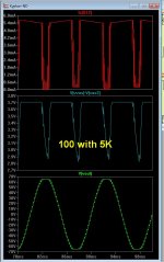
Dependent on frequency and the Z of the VAS when it clips.
(below) shows this effect.
At 5 hz , we do go into a "collapse" ... but we are clipping ,
who cares. Nothing to worry about - amp and speakers typically survive.
I realized this years ago , combined it with real world solutions.
The shunt R at the VAS and the spreader bypass cap determines what freq.
the "collapse" happens at.
Last post in this thread .... between the bickering and being ignored
despite very good contributions - I give up.
OS
Hi OS,
Nice pix. "collapse" is of course a matter of degree. Looks like the 1kHz curve has "collapsed" by about 200mV, meaning that at that point in time the output stage is way under-biased. Maybe it doesn't matter. Maybe the recovery is quick enough anyway. Of course, a deep collapse caused by a 20Hz clip will take longer to recover to the point of reasonable output stage bias - maybe for the sound of a higher frequency like 1kHz going through at the same time. What were the values of the VAS bypass capacitor and total resistance of the Vbe multiplier divider for these pix?
Sorry for the bickering distractions. Your excellent contributions have absolutely not been ignored, and I have appreciated them. I'm guessing that when most of the folks agree with you, you may not get many posts in response. I thank you for all of your contributions and hope you will stay.
Cheers,
Bob
Exactly as I did when deciding on the best diode arrangement in my Leach back in 2006. But P297 of your excellent book, halfway down the fourth paragraph, you mention waiting 20 secs before taking that measurement. I could never understand this.
And I think there are a couple of maths errors on page 322, lines 2 and 3 (if it hasn't already been mentioned).
Brian
Hi Brian,
Thanks for the feedback. I'll have to go take another look at that and try to figure out what I had in mind in waiting 20 seconds. In any case, if it has created any confusion it needs a bit of clarification in the second edition.
Cheers,
Bob
Writing a book and getting into selling kits and designs assumes, of course, different levels of responsibility for the target customers. I believe what Mr. Self does is about putting the money where his mouth is.
I would not like to be in the business of selling audio kits, and then being responsible for all human smoke generators with a soldering iron and a missing ohm law under the belt mishaps. Much easier is to stay on the fence and simulate circuits, you then will have all the time in the world to help the DIY community (and then look like a true guru).
I agree , I did review the compact blameless , load invariant before I even
did the Badger. Builders of those kits should not be "smoke generators".
Even on non-profit forum projects , one project "smoked" by a poor design
can be a last project (by the designer). Feedback by "picky" builders
is important to over-design the project so only user error is a factor.
Some will under-compensate , overload , or even "smoke" an amp
on purpose just to see HOW it might actually fail. 😀
PS - the simulator is especially useful to fine tune the design at
the prototype-builder "feedback stage" .
OS
Hi Waly,
Please re-read what I suggested, offer the gerber and bom and that is it. It really does not have to be complicated by these authors doing anything else.
OS for your point because we are talking hi V and I yes smoke is easy, if it was a 3.3V mcu ckt, the argument DNA. Having smoke is all part of the learning experience 🙂
I would think that one of the intentions of these books is so that one can build a pcb from them? and not having to resort to buying one already done for them. How are you learning to design a power amp that way?
So now you can design a power amp on paper, now build one, test it, critique it, that is the fun in it all and the learning experience.
Are these designers, ones that throw the schematic/design over the wall to the layout group and hope and pray they get a good layout. What a joke that is in the real world!! I hope that they set up all their design constraints correctly and that the parasitic in the back-annotations run well in the spice sims 🙂
Please re-read what I suggested, offer the gerber and bom and that is it. It really does not have to be complicated by these authors doing anything else.
I do not know which is worse, to sit on the fence or profit and offer the DIY community zip.Much easier is to stay on the fence and simulate circuits, you then will have all the time in the world to help the DIY community (and then look like a true guru).
OS for your point because we are talking hi V and I yes smoke is easy, if it was a 3.3V mcu ckt, the argument DNA. Having smoke is all part of the learning experience 🙂
I would think that one of the intentions of these books is so that one can build a pcb from them? and not having to resort to buying one already done for them. How are you learning to design a power amp that way?
So now you can design a power amp on paper, now build one, test it, critique it, that is the fun in it all and the learning experience.
Are these designers, ones that throw the schematic/design over the wall to the layout group and hope and pray they get a good layout. What a joke that is in the real world!! I hope that they set up all their design constraints correctly and that the parasitic in the back-annotations run well in the spice sims 🙂
Last edited:
Hi OS,
Nice pix. "collapse" is of course a matter of degree. Looks like the 1kHz curve has "collapsed" by about 200mV, meaning that at that point in time the output stage is way under-biased. Maybe it doesn't matter. Maybe the recovery is quick enough anyway. Of course, a deep collapse caused by a 20Hz clip will take longer to recover to the point of reasonable output stage bias - maybe for the sound of a higher frequency like 1kHz going through at the same time. What were the values of the VAS bypass capacitor and total resistance of the Vbe multiplier divider for these pix?
Sorry for the bickering distractions. Your excellent contributions have absolutely not been ignored, and I have appreciated them. I'm guessing that when most of the folks agree with you, you may not get many posts in response. I thank you for all of your contributions and hope you will stay.
Cheers,
Bob
Thanks , Bob.
The "collapse" simulations are with a 1uf bypass.
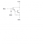
"testpig" (below pix) shows the standard spreader.
"A" is the Locanthi configuration.
"B" options are for an EF2 IRFP OPS.
I was thinking about a project associated with your book.
You are most famous for your old "HEC" OPS.
(attached PDF below) is what one member "morphed it" into.
I have the original simulation based on your paper and (a simulation)
of this one.
The attached one is very promising. Our member LKA has built it , as well.
It brings many of my IPS's solidly into the sub PPM realm !!
OS
Attachments
Question ----
The two legs of the spreader (sounds obscene) are bypassed.... I usually use a very large value, in the past, no sim.... just thought that the DC voltage across the C (Vbias) charges that cap and will help to maintain the DC bias level at a fixed/constant level.... pro-con to doing this ref. thermals ???
THx-RNMarsh
I agree, I think that the closer you get to a battery for the bias spreader the better (apart from the fact that it needs to be deliberately temperature dependent). A very large capacitor (1000uF) will cause a bit of a delay in output stage bias being applied at turn-on, but that should be no problem.
One thing always to bear in mind, however, is that while the amplitude of the bias disturbance from a clip interval will be smaller, the recovery time will have a longer tail. But if enough capacitance is used to, say, limit the bias spreader droop from a clip interval at the lowest frequency of interest to 13mV per RE (i.e., 26mV total), then one at least will not see the output stage being completely without workable bias for any interval.
Cheers,
Bob
- Home
- Amplifiers
- Solid State
- Bob Cordell's Power amplifier book