
LN super matched pairs such as SSM2212 have a low Vce(max) of 40V, not suitable for BC-1 AFE design specifying a supply of >= +/-55V
Super LN devices are not required, the noise is low enough using 2N5401. Hand selection of 2N5401 measuring Vbe of <= 1-2mV is sufficient for low DC offset.
The beauty of the BC-1 design is the performance for its simplicity, no need to make it anymore complicated, as imo little to be gained.
You have to be careful with the Pd on the SOT-363 vs the SSOT-6 package, plus the SSOT-6 is easier to solder.
I do a fair bit of smd soldering, I do not use a stencil and paste, I use AIM 15mil glowcore Eutectic no-clean solder, Mouser 738-13368
SSOT-6 has limited availability ATM - just 3 PNP, none matched. Thanks for the solder recommendation. I gave up on soldering surface mount with an iron long ago while doing rework on 0402 parts. It's just so easy with anything 0603 and larger to use paste and a hot air tool. I've been a digital guy for most of my career so I appreciate the insights into analog I get from this group.
Mouser has lots of FMBM5401 and FMBM5551 in stockSSOT-6 has limited availability ATM - just 3 PNP, none matched.
To each their own on methods when it comes down to smd soldering
That's right! I use normal solder, and sometimes liquid solder flux. I have to hold the smaller parts down. A glue stick also works well, but once you heat that up it becomes more permanent!
What about using MOSFETs likeExactly right, Mark. Using a MOSFET as a driver pretty much eliminates the need for a three-stage output stage. You are also correct in pointing out that the Cgd of the MOSFET driver is the main thing in play there, and to look out for.
It is also worth pointing out that safe operating area of the drivers, especially in big amplifiers, must also be adequate. MOSFETs as drivers can help in this way as well.
Speaking of capacitance to be driven by the VAS, and returning to all-BJT output stages, if we choose BJT drivers with enough SOA to drive a good-sized output stage, the Ccb of the drivers might be a little more than we would like for loading the VAS. Here we have another good case for a triple, where we can use a smaller pre-driver transistor, often of the same type of device as the VAS.
Cheers,
Bob
IRF9510, Qg=8.7, Ciss=200pF
IRF510, Qg=8.3, Ciss=180pF
for drivers?
Is 200pF still too much for the VAS to drive?
I have purchased the book and it serves me as a great reference for amplifier design and build. Thank you Bob for your work and contribution to the field.
I am still learning about EF3 OPS and have a few questions.
Would it make sense to use EF3 OPS for the amplifier with 37V-0-37V power supply voltage?
EF2 seems to be a tried and true stable version.
Using driver and two pairs of output transistors (EF2-2) delivers great results in simulation.
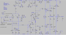
Amplifier in question is simple blameless concept with:
I am still learning and compensation parts like lead cap and RC networks across LTP and VAS output will need to be adjusted to correct values. Seems that I got two pole compensation along with LTP degeneration resistors adjusted correctly by using miller cap of 47p, and later series of 330p and 56p caps for TPC. What is interesting, I simulated and probed collector currents for driver transistors and adding speedup cap actually required drivers to be run at 2mA more current.
Thank you for your help!
I am still learning about EF3 OPS and have a few questions.
Would it make sense to use EF3 OPS for the amplifier with 37V-0-37V power supply voltage?
EF2 seems to be a tried and true stable version.
Using driver and two pairs of output transistors (EF2-2) delivers great results in simulation.
Amplifier in question is simple blameless concept with:
- two transistors LTP - FMBM5401, each at 2mA
- three transistors current mirror with helper transistor - FMBM5551,
- CFP constant current sources for LTP and VAS - PZT4403,
- emitter follower VAS - MMBT5551 + PZT4401 biased at 6.5mA
- two pole compensation
- driver transistors KSA1381 and KSC3503 biased at 9.2mA
- two pairs of output transistors - MJW1302 and MJW3281
I am still learning and compensation parts like lead cap and RC networks across LTP and VAS output will need to be adjusted to correct values. Seems that I got two pole compensation along with LTP degeneration resistors adjusted correctly by using miller cap of 47p, and later series of 330p and 56p caps for TPC. What is interesting, I simulated and probed collector currents for driver transistors and adding speedup cap actually required drivers to be run at 2mA more current.
Thank you for your help!
Attachments


this means you will have to run your VAS with more collector current otherwise...What about using MOSFETs like
IRF9510, Qg=8.7, Ciss=200pF
IRF510, Qg=8.3, Ciss=180pF
for drivers?
Is 200pF still too much for the VAS to drive?
What about using MOSFETs like
IRF9510, Qg=8.7, Ciss=200pF
IRF510, Qg=8.3, Ciss=180pF
for drivers?
When the configuration is source follower, the Ciss is effectively bootstrapped and hence relatively insignificant. The Crss is the one to watch out for. But Bob already said that just he called it Cgd which is the same thing.
input capacitance, Ciss = Cgd + Cgs
and for completeness:
reverse transfer capacitance, Crss = Cgd
output capacitance, Coss = Cds + Cgd
and for completeness:
reverse transfer capacitance, Crss = Cgd
output capacitance, Coss = Cds + Cgd
Depending on the slew rate you need you may need a lot more current to drive a powerFET. The capacitance is not linear and when driving them as switches there is a point where you need more current than seems correct. The capacitance chage is pretty significant and chages with source drain and source gate voltage, which are all changing. The models in the simulations are sim0lified and usually work but I would add more current. It alsways helps overall linearity anyway.
I always drive the output FETs with driver FETs. It worked well. There is also the really wide bandwidth to manage- you can have the devices oscillationg independent of the surrounding circuits.
I always drive the output FETs with driver FETs. It worked well. There is also the really wide bandwidth to manage- you can have the devices oscillationg independent of the surrounding circuits.
This is a better explanaion of the challenges than I could craft: https://toshiba.semicon-storage.com/info/application_note_en_20180726_AKX00068.pdf?did=59460
Hi Demian,
Yes, Gate Charge was also in some IR application notes. This is very often completely overlooked by designers.
-Chris
Yes, Gate Charge was also in some IR application notes. This is very often completely overlooked by designers.
-Chris
Yes, but because the junction is normally forward bias when it is active the changes are not as severe. You do still have to suck the charge out when turning it off.
Suffice to say all active devices need to have proper drive no matter the technology. Tubes are easier in that regard.
Suffice to say all active devices need to have proper drive no matter the technology. Tubes are easier in that regard.
Hello Bob, I've purchased your book, it's an excellent reference. The only thing that lets it down in my opinion is the rather sparse indexing. Is there a PDF version for verified purchasers so that we can search for terms?
Many people, including me, are wary of common emitter (or common source) output stages for power amps driving 4 ohm loads, because the open loop output impedance is so high. Nevertheless David Hafler did sell the TransNova power amp (description here) and some people really liked it. I believe some of Nelson Pass's class A Firstwatt amplifiers use common source output stages as well.
And I suppose you can say that an output stage using CFP / Sziklai connected devices, is a kind of common emitter amplifier with lots of local feedback applied -- but it only swings up to (Vrail - 2VBE), while a true common emitter output stage would swing to (Vrail - 0.5VBE) or so.
I'd like to read this ( history-of-the-transnova.pdf ). If anyone has the document saved, please upload here!
Thanks,
Alex
Like so much else, archive.org has it saved.I'd like to read this ( history-of-the-transnova.pdf ). If anyone has the document saved, please upload here!
Thanks,
Alex
https://web.archive.org/web/20190303161728/https://www.hafler.com/pdf/history-of-the-transnova.pdf
- Home
- Amplifiers
- Solid State
- Bob Cordell's Power amplifier book