We must be talking past one another here. I'm talking about thermal stability, i.e, stability of the bias current vs temperature and beta.. I think you must be talking about the stability of the Oliver point, or something.
The fact that you keep bringing up Gm, a small-signal parameter, while discussing thermal bias stability is a key to my confusion about what you are talking about. I recognize that Oliver gives you a context for equating DC and small-signal parameters, but I think you are extending it past the context.
Yes, I suppose I am, to make the explanation easier. 0.22 ohms emitter degeneration helps the thermal situation at idle current, but not much. Those really just help the sharing with high load currents.
Setting RE to get the Oliver condition is good for distortion, but thermal stability is mostly independent of the Oliver condition, and thermal bias stability is necessary to maintain the Oliver condition.
The fact that you keep bringing up Gm, a small-signal parameter, while discussing thermal bias stability is a key to my confusion about what you are talking about. I recognize that Oliver gives you a context for equating DC and small-signal parameters, but I think you are extending it past the context.
You are assuming that the voltage difference appears directly across Vbe and there is no degeneration.
Yes, I suppose I am, to make the explanation easier. 0.22 ohms emitter degeneration helps the thermal situation at idle current, but not much. Those really just help the sharing with high load currents.
Setting RE to get the Oliver condition is good for distortion, but thermal stability is mostly independent of the Oliver condition, and thermal bias stability is necessary to maintain the Oliver condition.
Heat decreases Vbe, This sentence might make sense in context but be wary of writing apparent contradictions.
You're right. I meant to write lower Vbe, or higher Ic, but didn't catch my error in the quick proofread.
--Russell
I think Bob is correct. The extra gain of a hot transistor reduces the base current and therefore the base resistor voltage drop and higher base voltage. Put another way, a cold transistor draws more base current and therefore the base resistor has more effect reducing current. In short, a base resistor exaggerates the tendency of a hot transistor to conduct more. You can simulate this with spice.
Hi Sandro,Since I have a bit of time, I'll pitch in:...
Nice to have you back. I've been missing your input.
Cheers, Ian
We must be talking past one another here. I'm talking about thermal stability, i.e, stability of the bias current vs temperature and beta.. I think you must be talking about the stability of the Oliver point, or something.
Usually it's me talking past everyone else because I think I'm smarter. Sometimes if it's confusing to follow it's just because I am tying myself up in knots. My mental state is really not that good.
The fact that you keep bringing up Gm, a small-signal parameter, while discussing thermal bias stability is a key to my confusion about what you are talking about. I recognize that Oliver gives you a context for equating DC and small-signal parameters, but I think you are extending it past the context.
I am using the Oliver condition as a way to keep apples to apples comparisons even though no one is being forced to use it. This is because Rb increases Ic tempco at the same time as reducing it by acting on Gm. The Oliver condition simplifies the relationship by keeping Gm constant regardless of Rb (by balancing it with Re), and the Oliver condition is more relevant to EF output design than an EF where we just increase the degeneration regardless of distortion. The point is relevance. If you violate the Oliver criteria you lose relevance to our goal which is a linear EF stage.
Setting RE to get the Oliver condition is good for distortion, but thermal stability is mostly independent of the Oliver condition, and thermal bias stability is necessary to maintain the Oliver condition.
Thermal stability is determined by thermal gain, which is determined by Ic tempco. Ic tempco is determined by Vbe tempco and Gm. If we weren't concerned with distortion or output swing, Gm could be anything. But we want the solution that gets us closest to the optimal bias which is the Oliver point.
We are not looking for a solution to thermal instability in a single emitter follower in class A, but for a complimentary EF in class AB with multiple parallel transistors. for which the goal of linearity will keep us from straying too far from the Oliver null point.
The first thing to do is to find out if we can satisfy Oliver while still being thermally stable - this is the most relevant to all of our goals. It doesn't make sense to give up on that goal just to prove that a base resistor would improve thermal stability, and ignore Oliver.
So while the Oliver condition may seem on the surface to be an arbitrary constraint, it is actually a useful tool for bringing our goals together so that it is not just a game of whack-a-mole.
Rb may help you reach the Oliver point at a lower current, and it may help your rf stability, but it hurts your DC and thermal stability.
Gm has everything to do with current hogging which is not compensated by the Vbe multiplier, and this can be shown in simulation. If you have for instance 2 2SC4793 in parallel as drivers then in certain conditions you can get one turning off due to differential thermal gain between them. The same can also happen with TO92 BJTs in parallel at high Vce. It can also happen in highly parallel high current BJT input stages used in some phono preamps. The same applies to the output transistors but to a lesser extent because they are more thermally optimized. And finally we know this phenomenon on the silicon level as hot spots forming in power BJTs during secondary breakdown.
I never argued that Rb should be increased to get to the Oliver point. I would argue that you may want to decrease Re to meet the Oliver criteria if the base resistance is set by necessity for stability. So on that point we agree.
I never argued that Rb should be increased to get to the Oliver point. I would argue that you may want to decrease Re to meet the Oliver criteria if the base resistance is set by necessity for stability. So on that point we agree.
Now I can see that we were, in fact, talking past each other. I agree with all those statements.
Gm has everything to do with current hogging which is not compensated by the Vbe multiplier, and this can be shown in simulation. If you have for instance 2 2SC4793 in parallel as drivers then in certain conditions you can get one turning off due to differential thermal gain between them. The same can also happen with TO92 BJTs in parallel at high Vce. It can also happen in highly parallel high current BJT input stages used in some phono preamps. The same applies to the output transistors but to a lesser extent because they are more thermally optimized. And finally we know this phenomenon on the silicon level as hot spots forming in power BJTs during secondary breakdown.
I never argued that Rb should be increased to get to the Oliver point. I would argue that you may want to decrease Re to meet the Oliver criteria if the base resistance is set by necessity for stability. So on that point we agree.
Yes, in many of my designs with paralleled output transistors I use 0.22-ohm emitter resistors and 2.2-ohm base stoppers, and get to the Oliver criteria with about 20 mV across the emitter resistors (as opposed to the theoretical 26 mV at room temperature).
Cheers,
Bob
@All,
BTW a spreadsheet for a basic push-pull BJT Follower output stage wingspread plots is available here What causes BJT based amplifier distortion?
It is for a simple NPN/PNP pair as a Follower with voltage drive.
I found the wingspread plot is quite sensitive to Re mismatch.
I found changing the Beta match from 100 each to 100/150 does not have much effect on the wingspread plot.
Similarly not much effect changing the IS matching.
BTW I believe Oliver's condition is met when bias factor Kb=1 ( 1*26mV above Vk).
And you don't have to learn to use a simulator to use this spreadsheet😉.
Hi Bob,
Here's the link for a DoubleCross(TM) spreadsheet for the Follower:
PAK412-Spreadsheet-DoubleCross-CC-wingspread.xls - Google Drive

.
Use 0.22 ohm and 0.18 ohm emitter resistors that you suggest in your book and with 290mA bias there is a relatively wide near zero distortion region up to a few watts.
Of course a practical amp bias will drift with varying signal levels of music so I don't have any idea yet how low the distortion can be maintained in a practical amp.
I saw a few posts ago your BC-1 build will have DoubleCross(TM) so you maybe able to get some figures soon. I'm looking forward it.
Cheers, Ian
Here's the link for a DoubleCross(TM) spreadsheet for the Follower:
PAK412-Spreadsheet-DoubleCross-CC-wingspread.xls - Google Drive
.
Use 0.22 ohm and 0.18 ohm emitter resistors that you suggest in your book and with 290mA bias there is a relatively wide near zero distortion region up to a few watts.
Of course a practical amp bias will drift with varying signal levels of music so I don't have any idea yet how low the distortion can be maintained in a practical amp.
I saw a few posts ago your BC-1 build will have DoubleCross(TM) so you maybe able to get some figures soon. I'm looking forward it.
Cheers, Ian
Attachments


Hi Bob,
Here's the link for a DoubleCross(TM) spreadsheet for the Follower:
PAK412-Spreadsheet-DoubleCross-CC-wingspread.xls - Google Drive
.
Use 0.22 ohm and 0.18 ohm emitter resistors that you suggest in your book and with 290mA bias there is a relatively wide near zero distortion region up to a few watts.
Of course a practical amp bias will drift with varying signal levels of music so I don't have any idea yet how low the distortion can be maintained in a practical amp.
I saw a few posts ago your BC-1 build will have DoubleCross(TM) so you maybe able to get some figures soon. I'm looking forward it.
Cheers, Ian
Hi Ian,
Yes, the BC-1 has a very simplified capability for approximating the DoubleCross output stage, but it is still experimental. The approach is to just include a base-to-base resistor on one of the output pairs to reduce its bias so that it begins to turn on as its opposite-sex device in the other pair begins to turn off. The conventional BC-1 has 2.2-ohm base stoppers in the output pairs. In the DoubleCross version, the base stoppers for the pair with the base-to-base bias attenuation resistor are 4.7 ohms so that the desired reduction in bias for that pair can be accomplished without using as much current as would otherwise be required if the base stoppers remained at 2.2 ohms for that pair.
Board availability for the BC-1 was delayed substantially by the effort on the DH-220C and a physical design change to the BC-1 boards to make them more compatible with available enclosures. Prototypes for those new boards are now being assembled for testing.
Cheers,
Bob
Hi Bob,
Nice to hear from you. My sims used 80mV for he tension bias (3*Vt). For 80mV across the base stopper there needs to be 17mA. Double that for two pairs. So I see the need for 5 ohms base stopper rather than 2 ohms.
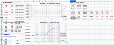
If you (or anyone) are interested the spreadsheet now has a section added to calculate THD as a function of input swing Vin and hence output power (ss link in earlier post).

I tried to get the same THD as LTspice for the same settings as the spreadsheet but the lower Vin THD calculations are lower than LTspice. There may be something I have overlooked, but so far the shape of the THD graph follows LTspice THD vs power plot which is a good start. I calculate THD first by finding the average gain for any Vin swing (as a running-average), then I find the deviation for each Vin increment up to Vin, and then average that from Vin=0 to Vin to give the ratio of distortion to the total signal for any Vin sinewave swing.
The xls version also runs with Solver so you can goal seek. I made RE14, Vb and VbT variables and chose the cell THD at Vin=10V as the value to be minimized. It returned a lower value changing RE14 from 0.18 to 0.194 ohms and Vb and VbT. It took 0.1 seconds to optimize (a log can be exported to an added sheet). The gain plot went from flat between -5V to +5V to wavy-flatish between -10V to +10V - a relatively low THD up to 6 watts.
Solver is very useful for biasing strategies for DoubleCross. There are so many more variables with DoubleCross than the simple two pair output stage making it almost impossible to find the best resistor values and best biasing with say LTspice.
And "best biasing" depends on whether you want higher order harmonics need minimizing (for best amp quality) or if unweighted THD is sufficient. At present Solver doesn't minimize higher order harmonics. But it's a good start. Enjoy🙂
To add Solver to Excel enter Solver in Excel Help and follow the instructions. It then comes up under Data>Analysis. Enter the cell reference to optimize and then the cells to change, eg RE14, Vb and VbT on Sheet 1) then Solve. Look at the new values and accept changes. I used Solver's default engine.
Nice to hear from you. My sims used 80mV for he tension bias (3*Vt). For 80mV across the base stopper there needs to be 17mA. Double that for two pairs. So I see the need for 5 ohms base stopper rather than 2 ohms.
If you (or anyone) are interested the spreadsheet now has a section added to calculate THD as a function of input swing Vin and hence output power (ss link in earlier post).
I tried to get the same THD as LTspice for the same settings as the spreadsheet but the lower Vin THD calculations are lower than LTspice. There may be something I have overlooked, but so far the shape of the THD graph follows LTspice THD vs power plot which is a good start. I calculate THD first by finding the average gain for any Vin swing (as a running-average), then I find the deviation for each Vin increment up to Vin, and then average that from Vin=0 to Vin to give the ratio of distortion to the total signal for any Vin sinewave swing.
The xls version also runs with Solver so you can goal seek. I made RE14, Vb and VbT variables and chose the cell THD at Vin=10V as the value to be minimized. It returned a lower value changing RE14 from 0.18 to 0.194 ohms and Vb and VbT. It took 0.1 seconds to optimize (a log can be exported to an added sheet). The gain plot went from flat between -5V to +5V to wavy-flatish between -10V to +10V - a relatively low THD up to 6 watts.
Solver is very useful for biasing strategies for DoubleCross. There are so many more variables with DoubleCross than the simple two pair output stage making it almost impossible to find the best resistor values and best biasing with say LTspice.
And "best biasing" depends on whether you want higher order harmonics need minimizing (for best amp quality) or if unweighted THD is sufficient. At present Solver doesn't minimize higher order harmonics. But it's a good start. Enjoy🙂
To add Solver to Excel enter Solver in Excel Help and follow the instructions. It then comes up under Data>Analysis. Enter the cell reference to optimize and then the cells to change, eg RE14, Vb and VbT on Sheet 1) then Solve. Look at the new values and accept changes. I used Solver's default engine.
Attachments

Last edited:
Update
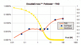
Hi Bob, All,
I have added compression of the spreadsheets calculated THD to conform with LTspice THD as shown (for the best flat region bias Kb=-0.27,KbT=3):

I chose to use "GmQ2+GmQ4" to compress the low-end THD where the two transistors contribute most of their gain and cause the low-end THD flat part. Using this is variable just a hunch, I need to check if it still gives reasonable THD estimates for other bias conditions.
I notice your 2nd Ed book has measured DoubleCross THD plots (Figs 13.11, 13.13 and 13.14) and the spreadsheet THD plots are similar - almost believable😉.
Both xls and ods spreadsheets have been updated on Google drive (links above). The xls version has Solver set up.
Hi Bob, All,
I have added compression of the spreadsheets calculated THD to conform with LTspice THD as shown (for the best flat region bias Kb=-0.27,KbT=3):
I chose to use "GmQ2+GmQ4" to compress the low-end THD where the two transistors contribute most of their gain and cause the low-end THD flat part. Using this is variable just a hunch, I need to check if it still gives reasonable THD estimates for other bias conditions.
I notice your 2nd Ed book has measured DoubleCross THD plots (Figs 13.11, 13.13 and 13.14) and the spreadsheet THD plots are similar - almost believable😉.
Both xls and ods spreadsheets have been updated on Google drive (links above). The xls version has Solver set up.
Attachments
Last edited:
Hi Ian,
This looks like really good work! Thank you! It is remarkable that you got results similar to actual measurements with a spreadsheet. That deserves a toast!
Its been almost a year since I worked on the first PCB prototype of the BC-1, having spent a great deal of time on the DH-220C. I am now in the process of stuffing the the next generation of BC-1 PCBs. Rick Savas and I did a major physical design change to make the boards more compatible with a nice 3U enclosure. We also made the design a bit more modular, with AFE (IPS/VAS),
OPS and protection (PROT) on 3 separate boards of equal height that will mount on the heatsink side of the enclosure. As soon as I get this BC-1 Rev. 2 up and running, I'll evaluate it in the DoubleCross mode and let you know the results. Rick has also designed a power supply board for the BC-1.
Best regards,
Bob
Hi Bob,
Nice. Maybe there is some way to do an A/B comparison while running like removing the link resistor between bases that removes the offset between pairs (and then re-bias for the ordinary optimum). maybe it would take some time for the heatsink temp to stabilise but still it might be helpful.
Thanks for a thumbs-up on the spreadsheet. One use for the DoubleCross spreadsheet is to find what biasing and emitter resistors gives the best linearity in the lower power region where distortion goes almost to zero before global feedback and up to a few watts. I have now used Sun's Solver engine with OpenOffice and used to to find values for the best linearity in the lower power region (as shown):

I have added another distortion metric which is the average deviation of the THD - it is averaged from Vin=0 up to my low power (Vin of 6 Vpk) - it gives a value for "waviness" in the wingspread low power region (I expect that relates to higher order harmonics which means more in audio amps than straight THD). Using this metric Solver tries to get the bias setting for the flattest gain in the low power region.
Using this approach I found the DoubleCross gave ten times lower distortion over the whole low power region than I was able to get by manually changing the bias values and the emitter resistor value for Q1,4.
Putting the new values into LTspice there was some improvement in linearity and THD.
So the spreadsheet with Solver optimisation is some help for designers of DoubleCross.
Cheers, Ian
As soon as I get this BC-1 Rev. 2 up and running, I'll evaluate it in the DoubleCross mode and let you know the results.
Nice. Maybe there is some way to do an A/B comparison while running like removing the link resistor between bases that removes the offset between pairs (and then re-bias for the ordinary optimum). maybe it would take some time for the heatsink temp to stabilise but still it might be helpful.
Thanks for a thumbs-up on the spreadsheet. One use for the DoubleCross spreadsheet is to find what biasing and emitter resistors gives the best linearity in the lower power region where distortion goes almost to zero before global feedback and up to a few watts. I have now used Sun's Solver engine with OpenOffice and used to to find values for the best linearity in the lower power region (as shown):
I have added another distortion metric which is the average deviation of the THD - it is averaged from Vin=0 up to my low power (Vin of 6 Vpk) - it gives a value for "waviness" in the wingspread low power region (I expect that relates to higher order harmonics which means more in audio amps than straight THD). Using this metric Solver tries to get the bias setting for the flattest gain in the low power region.
Using this approach I found the DoubleCross gave ten times lower distortion over the whole low power region than I was able to get by manually changing the bias values and the emitter resistor value for Q1,4.
Putting the new values into LTspice there was some improvement in linearity and THD.
So the spreadsheet with Solver optimisation is some help for designers of DoubleCross.
Cheers, Ian
Attachments
Hi Ian,
Cool stuff! Some of which is over my head 🙂.
I did most of my standard vs. DoubleCross comparisons with the heatsinks and everything in a settled quiescent bias state, and then did THD measurements in load bursts - meaning that the amplifier was run at a given voltage corresponding to a given test power with no load and the THD analyzer monitoring the no-load distortion and fully auto-tune stabilized, then I would connect the load briefly and take the THD measurement within a few seconds, basically the time it takes for the analyzer to settle.
Even this approach has some thermal shortcomings, since the long thermal time constant of the heat sink is not the only time constant in play. In particular, the time constant of Theta J-C is quite short - less than 100 ms.
Of course many of these same thermal time constant issues come into play and affect measurements on conventional output stages as well. Burst FFT distortion measurements with the QA401 may help in this regard.
One thing that is interesting when one biases the "ON" pair conducting the tension current is that they dissipate more and run hotter. As a result, their thermal swing is less between idle and periods of music that would other wise heat them up - they are already hot. They are operating closer to isothermal with varying power than in an ordinary class AB output stage, where dissipation is fairly low when optimally biased.
At the same time, the "OFF" pair is cooler. Their cases are pretty much at the same heat sink temperature as the "ON" devices with the exception of thermal drop across the insulator of the "ON" devices. Their average dissipation is low, so there is not much Theta J-C thermal drop. This all means that when the current hand-off at one of the displaced crossover points occurs, the hand-off is going from a hot transistor to a cold transistor. I think I've got that right. This is not necessarily a bad thing, it just needs to be taken into account. This complicates analysis a bit.
Cheers,
Bob
pedantry is beginning to emerge... Maybe I should just stick to answering questions.
pedantry = ANAL
PS - I also stand accused.
OS
- Home
- Amplifiers
- Solid State
- Bob Cordell's Power amplifier book