Yes it is excellent. I'm reading it at the moment.
I have found a typo on page 87 (Miller Compensation). In the example given , the reactance of C1 (33pf) at 20KHz is denoted (twice) as 24,000 ohms - instead of 240,000. However, it doesn't affect the end result of the linear gain calculation (500).
Apologies if this has already been pointed out.
Hi VHF man,
I'm glad you like my book and I really appreciate you pointing out errors. If you find any more, please don't hesitate to let me know.
Cheers,
Bob
ostripper ,
Does it? How many ideal values, how many mathematical constants, how many (missing) derivatives are employed in the bitter struggle against the uncertainty principle?The "fabulous world of simulation" can come scary close to the real thing provided the proper models.
jcx,
The larger capacitance, the more feedback, the greater linearity?"A significant aid in keeping the distortion contributed
by the final stage as low as possible is provided
by the compensation scheme, which exploits
the direct connection of the Miller capacitor
at the amplifier’s output to introduce a local AC
feedback path enclosing the output stage itself."
Edmond,
😀
You don`t say. Could it be me? Without even giving me a chance to provide substantial evidence and logic? How long is your ignore list?I just added three more people to my ignore list, as they are not only stone deaf to my arguments, but also prefer to speculate on alleged typos without any substantial evidence and logic.
😀
If we accept both of your statements as truths it requires the belief that Baxandall lacks the ability to select proper component values - something I find absurd given his obvious talent. This leads to my opinion that it was a typo.
So in one hand he s got huge talent, that lead to think that
he knows how to select adequate resistor value; and on the other
hand, this same talent lead him to make unprobable typos ?......
Reality is that the text is very well written, or rather copied
from a firstly hand written memo, so the "professor" had all
the necessary "recoil" to check for eventual mistakes.
The reason he s quoting a 68R return resistor lies elsewhere,
that is in the experience protocols itself.
Firstly, he says " a good deal higher than the OS output impedance"
which he says is about 20R at the frequencies of interest,
so that match the 68R value...
Secondly, he seems to set a necessary condition, that is implementing
a return path from the OS, as enough for the scheme to work,
without specifying another necessary condition that the
VAS has enough gain.
Therefore, for TMC to work, and badly , the said resistor must be low
enough to allow for a minimal NFB between the OS and VAS input.
Just make a sim using a non enhanced VAS and an enhanced
one, you ll see that the first mentioned has not enough gain
to make the TMC related THD reduction significant, using the
values we are now accustomed to.
Hence the low value resistor to increase the dominance
of the relevant NFB loop and make the effect audible
when experimenting with a zero bias OS.
That said, i agree that he did set a footstep on TMC
implementation possibility ,but unfortunately it was
develloped without his contribution since these papers
were not published in proper time to contribute the way
they should have been...
Last edited:
TO Bob Cordell
Hi Bob
I am repeating hereunder my post of a few days ago that you must have missed.
I am interested to have your comments because I find this if applicable a great protection system.
"
I have read your suggestion of using the left over TT diodes to detect the temp of the junction and protect the transistor before reaching let say 150°C. If we have such a detection coupled with a maximum current detector we are safe with respect to short circuit protetcion.
The question remaining is secondary breakdown. Do you believe that monitoring the power max temp is safe enough. Secondary breakdown will happen with some reactive loads but it has been shown elsewhere that derating for temp during secondary breakdown should be less stringeant than the derating of power dissipation because the effect of increase of emitter resistance with temperature. In other words, with increase in temperature, the normal power limit takes over the secondary breakdown limit for higher Vce than at lower temperature. If you couple this with the 10 ms SOA limit, is it not reasonnable to say that monitoring the 150°C crossing is totally safe for normall ( less than 45° phase) loads.
Then a totally non intrusive SOA protection device can be designed.
Looking at the data sheet of NJL3281 the 10ms SOA limit is fully power dissipation with no 2° breakdown sign. Is this not a good argument to design a protection sollely based on T° of junction ( for audio program). Unfortunatelly, there is no derating curves with temp but as said above, higher temperatures will shift the full limit to the left but the start of 2° breakdown will be, relatively to this shifted curve, shift to the right in the higher temp limiting curve.
The thermal attenuation between Transistor and diode must be taked into account on the safe side by estimating the transistor 150 °C beeing a lower temperature in the diode. Is your thermal model of TT good enough for this exercice.
"
Thanks
JPV
TMC discussion, wish it was a dedicated thread just to keep this one about Bob's book and to make it easier to find the TMC discussion.
Ditto
TT bias
Hi Bob,
No problem (of course).
That's exactly the info I needed. Thanks a lot!
You may omit the second Vbe multiplier when the base to base voltage of the O/P trannies is sensed (as in HEC) or when a diamond driver is used with the pre-drivers and main-drivers kept on the same (local) heat sink. In case of the latter, Vbe shifts of the driver components are 'automatically' compensated. Please, see also my latest bias scheme: http://www.diyaudio.com/forums/solid-state/174218-rebirth-phoenix-8.html#post2396672
Cheers,
E.
Hi Edmond,
I looked at the post and responded as here below. Thanks for bringing my attention to it.
Hi Edmond,
I'm sorry I'm late getting back to this post - I just lost track of this thread.
Hi Bob,
No problem (of course).
You are right about thermal attenuation within the ThermalTrak devices between the transistor junction and the tracking diode. This is certainly non-ideal, but the ThermalTrak arrangement is still far superior to the conventional arrangement, which suffers even more thermal attenuationa and far more thermal delay.
In general, some experimentation is needed in setting up the optimum compensation for a ThermalTrak amplifier. Some form of electrical multiplication usually has to take place in the Vbe multiplier associated with the ThermalTrak devices. Indeed, some multiplication is often needed anyway because the temperature coefficient of the ThermalTrak diodes is not quite the same as that of the BJT. So the needed amount of multiplication is all wrapped together the best we can.
In many cases I'll use two Vbe multipliers, one working with and incorporating the ThermalTrak tracking diodes and the other providing bias spreading for the remaining devices of the output Triple. That way, the amount of multiplication allocated to each process can be set somewhat independently. The transistor of the second Vbe multiplier usually wants to track the temperature of the pre-driver and driver transistors. Indeed, if the driver transistors happen to be mounted on the heat sink, then the transistor of the second Vbe multiplier may also be mounted on the heatsink.
That's exactly the info I needed. Thanks a lot!
It was a two Vbe multiplier arrangement like this that I used for the test amplifier whose bias behavior is shown in Figure 14.23 in the book. In that case, the second Vbe multiplier along with the pre-drivers and drivers were mounted on an isothermal bar/heatsink on the circuit board.
Cheers,
Bob
You may omit the second Vbe multiplier when the base to base voltage of the O/P trannies is sensed (as in HEC) or when a diamond driver is used with the pre-drivers and main-drivers kept on the same (local) heat sink. In case of the latter, Vbe shifts of the driver components are 'automatically' compensated. Please, see also my latest bias scheme: http://www.diyaudio.com/forums/solid-state/174218-rebirth-phoenix-8.html#post2396672
Cheers,
E.
ostripper ,
Does it? How many ideal values, how many mathematical constants, how many (missing) derivatives are employed in the bitter struggle against the uncertainty principle?
Hi WuYit,
How much experience have you had builing amplifiers and simulating them? It sounds like you are being a bit too negative on simulation. If you have had bad experiences, can you share them with us?
When the simulation is done properly with decent transistor models, and when the corresponding amplifier is built well (good wiring practices, good bypassing, no parasitic oscillations, solid design), the correspondence between simulation and the amplifier performance should be quite good.
Correspondence is never perfect because of real-world things that are usually not accounted for in simulation, such as wiring inductances, wiring capacitive or inductive coupling, etc. But in a decent execution of a design, these should be second-order in their effect, and are no reason to throw up one's hands and dismiss simulation results.
Cheers,
Bob
Let's smoke out the trolls
Hi Bob,
Did you know there exists something called 'ignore list' ? 😉
Cheers,
E.
Hi Bob,
Did you know there exists something called 'ignore list' ? 😉
Cheers,
E.
I found the Baxandall papers to be very "comforting" and easy to understand .. he must of been a great teacher. His observations are very similar to what I have experienced upon adoption.
Very true, I know exactly what you mean. I had a good deal of correspondence with Peter and he was unfailingly courteous and good-tempered, and always ready to explain a tricky point without a hint of ego or condescension. A great loss.
I am proud to re-confirm "I have never used the ignore facilities" of this Forum.there exists something called 'ignore list' ?
Hi JCX
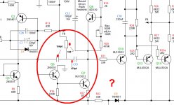
My copy of the datasheet just says "Schematic Diagram" and doesn't indicate that it has been simplified. As you say, capacitor C4, which certainly looks like a Miller cap to me, is fed from the final gain stage. It does not include the unity-gain output stage, so I don't think it counts as Cherry Inclusive compensation. Looks to me like a Nested Miller compensation scheme, which is very popular in four-stage opamps. (I'm counting the unity-gain output as a stage)
The R12 in series with C4 presumably implements some sort of pole-zero cancellation. Do others agree?
Well, that seems plain enough- pity we don't have a schematic. I strongly suspect that if we did, we would find it was an example of the commercial use of TMC. It also looks like an unconventional output stage, but that may be irrelevant.
The date on my TDA7293 datasheet is Dec 1999; does anyone know if that was when the chip was released?
the LT1028 datasheet shows the simplified internal circuit at the bottom, the over-compensation C is added from the output to the "final VAS" Q23 base - there is an "extra" diff pair gain stage in the middle so there are multiple compensation loops
My copy of the datasheet just says "Schematic Diagram" and doesn't indicate that it has been simplified. As you say, capacitor C4, which certainly looks like a Miller cap to me, is fed from the final gain stage. It does not include the unity-gain output stage, so I don't think it counts as Cherry Inclusive compensation. Looks to me like a Nested Miller compensation scheme, which is very popular in four-stage opamps. (I'm counting the unity-gain output as a stage)
The R12 in series with C4 presumably implements some sort of pole-zero cancellation. Do others agree?
the TDA7293/4 both have the text in the datasheet:
"A significant aid in keeping the distortion contributed
by the final stage as low as possible is provided
by the compensation scheme, which exploits
the direct connection of the Miller capacitor
at the amplifier’s output to introduce a local AC
feedback path enclosing the output stage itself."
Well, that seems plain enough- pity we don't have a schematic. I strongly suspect that if we did, we would find it was an example of the commercial use of TMC. It also looks like an unconventional output stage, but that may be irrelevant.
The date on my TDA7293 datasheet is Dec 1999; does anyone know if that was when the chip was released?
The 100V version datasheet (TDA7294) is dated feb 1996,
so it originate well before 1996.
Manufacturers are somewhat reluctant when it comes
to technical information about top products....
Last edited:
trolls
Then you must have a lot a patience, or a lot of time. 😉
I am proud to re-confirm "I have never used the ignore facilities" of this Forum.
Then you must have a lot a patience, or a lot of time. 😉
Hi Bob
I am repeating hereunder my post of a few days ago that you must have missed.
I am interested to have your comments because I find this if applicable a great protection system.
"
I have read your suggestion of using the left over TT diodes to detect the temp of the junction and protect the transistor before reaching let say 150°C. If we have such a detection coupled with a maximum current detector we are safe with respect to short circuit protetcion.
The question remaining is secondary breakdown. Do you believe that monitoring the power max temp is safe enough. Secondary breakdown will happen with some reactive loads but it has been shown elsewhere that derating for temp during secondary breakdown should be less stringeant than the derating of power dissipation because the effect of increase of emitter resistance with temperature. In other words, with increase in temperature, the normal power limit takes over the secondary breakdown limit for higher Vce than at lower temperature. If you couple this with the 10 ms SOA limit, is it not reasonnable to say that monitoring the 150°C crossing is totally safe for normall ( less than 45° phase) loads.
Then a totally non intrusive SOA protection device can be designed.
Looking at the data sheet of NJL3281 the 10ms SOA limit is fully power dissipation with no 2° breakdown sign. Is this not a good argument to design a protection sollely based on T° of junction ( for audio program). Unfortunatelly, there is no derating curves with temp but as said above, higher temperatures will shift the full limit to the left but the start of 2° breakdown will be, relatively to this shifted curve, shift to the right in the higher temp limiting curve.
The thermal attenuation between Transistor and diode must be taked into account on the safe side by estimating the transistor 150 °C beeing a lower temperature in the diode. Is your thermal model of TT good enough for this exercice.
"
Thanks
JPV
Hi JPV,
I apologize for missing that earlier post.
This is a tantalizingly interesting proposal. As you point out, I had previously thought of the extra ThermalTrak diodes as being useful for temperature monitoring, and thus as some sort of protection mechanism that might be a lot better than a thermal breaker mounted to the heat sink, for example. But I had not given any thought to the use of those sensing diodes as the central part of an SOA protection system.
Without giving it a lot of thought, I'm guessing that the 40 ms or so time constant between the junction and the sensing diode might be of concern. A lot can happen to bipolars in 40 ms.
As you correctly point out, the SOA derating with junction temperature does not always follow the same rule as for power derating. Maybe the sensing diodes can be used in some way to make a more conventional protection system less intrusive. For example, most V-I limiters do not take into account the power transistor junction temperature, so in some sense they should be designed to keep the transistors safe under worst-case pre-existing thermal conditions. One could argue that the more accurate thermal sensing afforded by the ThermalTrak diodes might be used to control to some extent the agressiveness of the V-I (or other) protection scheme.
I'm just not sure that the sensing diodes could be used alone as the central element of the protection scheme. On the other hand, we might look at it from the inverse point of view. There are those amplifier designers who essentially use no second-breakdown protection, relying solely on the beefiness of the output stage and brute-force short-circuit protection. These protection schemes are certainly not intrusive until a fuse is blown or the output stage is destroyed 🙂.
Although the use of the sensing diodes might not be as fast as we like, their use in some kind of protection scheme for such unprotected amplifiers might yield a worthwhile improvement in overall protection tradeoff.
The least intrusive protection is that which is never activated. This argues for beefy output stages and high thresholds, even when protection is used. Anything we can do to avoid premature or unnecessary activation of protection is helpful. Of course, it goes without saying that such protection schemes must add no degradation to the amplifier's operation when the are not protecting.
I hope this helps a bit, but I'll be the first to admit that I am being somewhat speculative here. People have written tomes on protection schemes.
Cheers,
Bob
Dear Bob Cordell.... my people (Brazilians) are excited about TMC
Your book was readed and also Baxandall texts.
I have just released a new model of amplifier (hundred boards sold in the group buy...half and half to brazilians and to the international comunitty) ... and i have a few guys that wants to try the modification.... when i am asking them to wait comparative tests i should make next year.
But, as i am very curious, i would like to ask if there's some audible effects... say...clear audible effect into a blind A to B comparison.... the question is a consequence of the distortion numbers...awsome numbers...but is this inside the human threshold of audibility?...can we easily perceive that?
I have some worries because my boards, recently released, have not been made to accept this modification... was not my prevision...so, they may produce very ugly connections to try, and many of them does not know how to compare...so..they may "follow the leader"....or what the leader said....in this case the leader is you.
My last amplifier is a modified Blameless, having bootstrap to feed VAS, enhanced VAS, or darlington VAS as you have shown... something alike Blameless with some steróids.
thank you in advance by your kindness to spend a couple of minutes with me..i will feel deeply honored by that... you are one of the most respected experts in our comunitty.... but also i know you love measurements..when i love to listen and evaluate.
regards,
Carlos
Attachments
Last edited:
My last amplifier is a modified Blameless, having bootstrap to feed VAS, enhanced VAS, or darlington VAS as you have shown... something alike Blameless with some steróids.
Adequate for the said compensation.
THD is significantly reduced..
Attachments
Hi JPV,
I apologize for missing that earlier post.
This is a tantalizingly interesting proposal. As you point out, I had previously thought of the extra ThermalTrak diodes as being useful for temperature monitoring, and thus as some sort of protection mechanism that might be a lot better than a thermal breaker mounted to the heat sink, for example. But I had not given any thought to the use of those sensing diodes as the central part of an SOA protection system.
Without giving it a lot of thought, I'm guessing that the 40 ms or so time constant between the junction and the sensing diode might be of concern. A lot can happen to bipolars in 40 ms.
As you correctly point out, the SOA derating with junction temperature does not always follow the same rule as for power derating. Maybe the sensing diodes can be used in some way to make a more conventional protection system less intrusive. For example, most V-I limiters do not take into account the power transistor junction temperature, so in some sense they should be designed to keep the transistors safe under worst-case pre-existing thermal conditions. One could argue that the more accurate thermal sensing afforded by the ThermalTrak diodes might be used to control to some extent the agressiveness of the V-I (or other) protection scheme.
I'm just not sure that the sensing diodes could be used alone as the central element of the protection scheme. On the other hand, we might look at it from the inverse point of view. There are those amplifier designers who essentially use no second-breakdown protection, relying solely on the beefiness of the output stage and brute-force short-circuit protection. These protection schemes are certainly not intrusive until a fuse is blown or the output stage is destroyed 🙂.
Although the use of the sensing diodes might not be as fast as we like, their use in some kind of protection scheme for such unprotected amplifiers might yield a worthwhile improvement in overall protection tradeoff.
The least intrusive protection is that which is never activated. This argues for beefy output stages and high thresholds, even when protection is used. Anything we can do to avoid premature or unnecessary activation of protection is helpful. Of course, it goes without saying that such protection schemes must add no degradation to the amplifier's operation when the are not protecting.
I hope this helps a bit, but I'll be the first to admit that I am being somewhat speculative here. People have written tomes on protection schemes.
Cheers,
Bob
Under short circuit, your flying catch diodes could keep the system with a fixed power dissipation until the junction reaches 150°C providing the time constants are right. Don't you think that this is a situation that can be accurately simulated using your TT thermal model.
If the short circuit aspect is solved, then one may design for a known load ( this is DIY ) by using a Zobel network that presents a near resistive load to the amplifier and there will be no 2° breakdown risk anymore ( see Leach model). Then the power only protection is enough
Is this correct?
A question on the operation of the flying catch diode ( fig 15.11 page 327)/
Is this a solution that has been tested in reality with BJT. Will it operate correctely whenever the short happens during any program signal with any phase, providing of course you can handle the limited power.
JPV
Your book was readed and also Baxandall texts.
I have just released a new model of amplifier (hundred boards sold in the group buy...half and half to brazilians and to the international comunitty) ... and i have a few guys that wants to try the modification.... when i am asking them to wait comparative tests i should make next year.
But, as i am very curious, i would like to ask if there's some audible effects... say...clear audible effect into a blind A to B comparison.... the question is a consequence of the distortion numbers...awsome numbers...but is this inside the human threshold of audibility?...can we easily perceive that?
I have some worries because my boards, recently released, have not been made to accept this modification... was not my prevision...so, they may produce very ugly connections to try, and many of them does not know how to compare...so..they may "follow the leader"....or what the leader said....in this case the leader is you.
My last amplifier is a modified Blameless, having bootstrap to feed VAS, enhanced VAS, or darlington VAS as you have shown... something alike Blameless with some steróids.
thank you in advance by your kindness to spend a couple of minutes with me..i will feel deeply honored by that... you are one of the most respected experts in our comunitty.... but also i know you love measurements..when i love to listen and evaluate.
regards,
Carlos
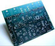
Hi Carlos,
Those are very nice looking boards!
TMC is certainly a very inexpensive and effective way to reduce distortion, particularly that arizing in the output stage. However, it is also fair to say that many well-designed BJT amplifiers can provide superb performance without TMC, so don't feel bad if you cannot use it. In any given amplifier development, I recommend that you temporarily compensate the amplifier both ways if you are going to consider TMC. Compensate it conventionally first, then compensate it with TMC. Look at THD-20 in each case. If the use of TMC does not improve the distortion numbers significantly, this may mean that the basic design of the amplifier, especially the IPS-VAS, can be improved, and I recommend tackling that first.
I have not done any comparative listening tests between the same amplifier compensated with and without TMC, and I honestly am not sure how much difference one could hear between the two if both are very well-designed.
As you know, I like MOSFET power amplifiers. However, due to transconductance droop, a MOSFET power amplifier with the same number of output pairs and idling at the same bias current will tend to have higher THD than a comparable BJT amplifier, at least in conventional bench tests. This was the reason I originally applied Hawksford Error Correction (HEC) to a MOSFET power amplifier - it did a wonderful job of mitigating the effects of transconductance droop. For similar reasons, I think TMC can be used to make the biggest difference in MOSFET power amplifiers; one then gets the benefits of MOSFETs and has THD-20 that is competitive with the best BJT amplifiers. One could always argue, of course, that one could apply TMC to a BJT amplifier and get still better THD performance.
There is, however, an argument that makes TMC very attractive for BJT amplifiers, and it may have little to do with static distortion measurements. It has more to do with what happens to crossover distortion under dynamic music conditions, where thermal bias mis-tracking may be poor, resulting in much worse crossover distortion than under static conditions (this is much less of a problem with MOSFETs). Here the use of TMC can mitigate some of the nasties of BJT output stages.
Cheers,
Bob
- Home
- Amplifiers
- Solid State
- Bob Cordell's Power amplifier book