I found the paper in question through Edmond Stuart's website, and I must say it is the best 12 pages I've read in a while.
Thank you for your kind words; I’m glad you found it useful. 🙂
To save others time finding it should they wish to read it, it is here:
tinyurl.com/TwoPoleCompensation-pdf
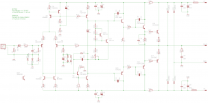
The schematic at figure 17 is similar to one in Cordell's book, and I have some reservations about enclosing three transistors in the miller loop. Is this stable in practice and are there any special precautions that need to be taken?
Could I check that you have read the version of the paper with an addendum (this appears as the final page of the PDF, after the conclusion)? Your question (along with other important issues) is addressed there.
Last edited:
Thank you for your kind words; I’m glad you found it useful. 🙂
To save others time finding it should they wish to read it, it is here:
tinyurl.com/TwoPoleCompensation-pdf
Could I check that you have read the version of the paper with an addendum (this appears as the final page of the PDF, after the conclusion)? Your question (along with other important issues) is addressed there.
Hi HarryDymond,
Thank you 🙂 for this very nice paper you did offer to us all 😀, and as did write Ranchu32, for me too : "I must say it is the best 12 pages I've read in a while". Very interesting paper.
Best regards
rephil
Thank you 🙂 for this very nice paper you did offer to us all 😀
Thanks also due to the Audio Engineering Society for allowing me to share it freely rather than making you all buy it from them!
...The schematic at figure 17 is similar to one in Cordell's book, and I have some reservations about enclosing three transistors in the miller loop.
I recall that the particular example in Bob's book was checked by Mike Kiwanuka (in this forum) and found to be unstable.
Apparently Bob had updated some of the transistor models but not rechecked stability for that circuit.
So you do need to be careful, especially since I think the Dymond example has four (The IPS cascode, EF in the VAS, the VAS, the VAS cascode.
Best wishes
David
Don’t forget that, being common-base, cascodes are “fast”. If a configuration is stable (with healthy margins) without cascodes, adding them will probably be OK (but of course this should be checked!!). Adding an emitter follower is the most likely thing to adversely affect stability margins. In any case, the miller loop can be compensated fairly easily with a small resistor and capacitor.
Hey guys,
Have you looked more at this circuit?
It's the extra output zobel at the speaker cable entrance to block RFI ingress:

Like his chipamp (pg 540 of Cordell's, Designing Audio Power Amplifiers, Fig 27.3 The Super Gain Clone Employing a DC Servo)
On pg 541, he writes:
------------------------------------------------
...
"Output Network
The output network is a pi-section arrangement with Zobel networks on both sides of the L-R network. This provides enhanced resistance to RFI ingress via the speaker cables. The inductor is optionally constructed as an air-core toroid to keep the magnetic field circulating largely inside the toroid, reducing possible magnetic coupling to other circuits. The first Zobel, comprising C and R, is located close to the output of the LM3886. The L-R network and second Zobel are located close to the speaker output terminals, optionally on a small separate board. The output signal is carried from the main board to the output network board by about 6 in. of high-quality speaker cable."
---------------------------------------------------
Any formulas, simulations, analysis ... ?
Cheers,
Jeff
http://www.diyaudio.com/forums/vend...er-achieving-0-0004-thd-n-64.html#post4167273
Have you looked more at this circuit?
It's the extra output zobel at the speaker cable entrance to block RFI ingress:
Like his chipamp (pg 540 of Cordell's, Designing Audio Power Amplifiers, Fig 27.3 The Super Gain Clone Employing a DC Servo)
On pg 541, he writes:
------------------------------------------------
...
"Output Network
The output network is a pi-section arrangement with Zobel networks on both sides of the L-R network. This provides enhanced resistance to RFI ingress via the speaker cables. The inductor is optionally constructed as an air-core toroid to keep the magnetic field circulating largely inside the toroid, reducing possible magnetic coupling to other circuits. The first Zobel, comprising C and R, is located close to the output of the LM3886. The L-R network and second Zobel are located close to the speaker output terminals, optionally on a small separate board. The output signal is carried from the main board to the output network board by about 6 in. of high-quality speaker cable."
---------------------------------------------------
Any formulas, simulations, analysis ... ?
Cheers,
Jeff
http://www.diyaudio.com/forums/vend...er-achieving-0-0004-thd-n-64.html#post4167273
Last edited:
I posted an excel.xls that shows the Dr Cherry analysis of the Thiele Network a few years ago.
http://www.diyaudio.com/forums/solid-state/94029-when-output-inductor-needed.html#post1105724
I started looking at the Pi Network a few years after I read the original '97 article and now adopt regularly.
http://www.diyaudio.com/forums/solid-state/94029-when-output-inductor-needed.html#post1105724
I started looking at the Pi Network a few years after I read the original '97 article and now adopt regularly.
Last edited:
... common-base, cascodes are “fast”.
Hi Harry
Yes they are "fast" but I am not sure how much this helps.
My intuitive feel is that if we keep the outer loop return ratio the same then the added cascodes must push up the return ratio of the inner loop.
But this stuff isn't always intuitive so I have started to look at inner loop stability, as part of a study of Two Pole Compensation.
Do you have any references to work on inner loop stability?
Principles are the same of course, but plots of outer loop Return Ratio are so common that the inner loop looks "funny" by comparison.
Especially since it is often implicitly assumed that the inner loop has no poles at all.
Best wishes
David
"But I have found them to be absolutely hopeless in an EF3 configuration: the only way to stabilise the thing was to drop the ULGF to ~250kHz or slug the drivers with a heavy Cbc. I believe there has been angst amongst some of the builders in the EF3 Slewmaster thread and some of their findings correlate with my own."
I used the 21193/4 in my Ovation 250 and despite their low fT the amp sounds very good to my ears. I am using a triple config in that amp with no problems. I've used base stoppers on the output devices and an RC stopper in the driver bases. If TMC comp'd the a Ovation 250.
I think 500 kHz ULGF with those output trannies is about right for a triple. You may be able to get a bit more with an EF2.
Hi Bonsai
I'm looking at your schematic now and see a 30 MHz driver with a B-C zobel @ ~6 MHz and a small base stopper. Can you explain how you arrived at these values or was it a case of trial and error.
I suspect I'm still getting some minor parasitic oscillation on my amp (the heatsink is warmer than I would expect) although I can't see anything obvious on the scope trace (a 100MHz Tek CRO).
Attachments
Hi Bob
The examples in your book (I'm referring to the schematics in Chapter 3 specifically) all feature very high LTP degeneration (470R emitter resistors) and a 1mA tail current, which is relatively low for a degenerated LTP.
Self on the other hand runs the LTP much hotter at approx 4mA and I suspect would run them even hotter if the packages permitted. He suggests 68-100 Re as a practical compromise between LTP linearity and voltage noise in the degen resisters at those currents.
Bonsai from these forums takes it to the extreme and runs the LTP super hot @ ~10mA
In my circuits I try to keep TO-92 Pd to < 100mW or thereabouts, since any higher and the device feels too hot to the touch. That correlates approximately with Self's examples.
Intuitively, I would think the tail current should be as high as practical (appropriately degenerated) to maximise drive into Cdom.
Can you shed any light on your philosophy?
Cheers
Christian
Hi Christian,
You have asked a very good question, and one that has obviously sparked some good discussion here. There are no black-and-white answers here, and many of the replies subsequent to your post are quite good.
Like many engineers, I have my own comfort-zone rules of thumb, and sometimes we do not venture outside these zones as much as we should dare.
That having been said, and particularly for the examples in Chapter 3, here is some of my rationale and sometimes slightly arbitrary choices. First, when in doubt with a CE BJT stage, I always like to use 10:1 degeneration. This gives good linearity. If I am running a transistor at 1mA, this means that re of the transistor will be about 26 ohms and the degeneration resistor will be about 260 ohms. Actually that is probably 11:1 degeneration in terms of gain reduction. I also like to keep Miller compensation capacitors in the range of 30pF plus or minus a factor of 2. I think I had 30pF in most instances in Chapter 3. The amplifiers in Chapter 3 usually had fairly conservative compensation with ULGF of about 500kHz. These personal rules of thumb of mine tend to work together with these various numbers.
Of course, whether we use a current mirror load on the IPS (which I usually do) influences this because it doubles the gm of the IPS. Also, the sweet spot for Cmiller is also influenced by whether a VAS is used that includes a Darlington (which I usually do). The Darlington VAS largely kills the nonlinear Cbc effect of the VAS transistor, permitting use of a smaller Miller comp capacitor.
This is admittedly somewhat arbitrary hand-waiving. I also shy away from passing a lot of current through an early stage when not needed.
A 2mA tail with each input transistor at 1mA provides peak current of 2mA into Cc if a current mirror is used. 2mA into a 30pF Cc yields 60V/us, a reasonable number for many amps, especially when it is achieved in a linear way, as with 10:1 degeneration.
If we want to go to higher ULGF and keep the same Cc, we will likely double the tail current and IPS gm to get to, say, 1MHz (rather than going down to 15pF for Cc. But this is just a judgment call.
Now to noise. This is indeed a possible objection to operating the IPS transistors at only 1mA and with a full 10:1 emitter degeneration. Some folks are obsessed with low noise, even in a case where signals are line-level. Don't get me wrong, I like low noise as well. IPS gm and degeneration do affect noise, including that which is input-referred from later stages like the VAS. I like to have a power amplifier input noise below 10nV/rt Hz, and consider 5 nV/rt Hz to be really good. If you look at the sub-section labeled "Noise of a degenerated LTP on page 152 you'll see some back-of-the-envelope numbers that show that a 2mA tail and 10:1 degeneration delivers about 5nV/rt Hz without considering later stages.
I guess the bottom line is that in the kinds of designs I do, I don't see much important advantage of running the IPS hotter than a tail of 2mA in designs with ULGF in the 500kHz - 1MHz range. Running the IPS hotter doesn't hurt, especially in amps with higher ULGF or SR targets as long as impedances in the base circuits of the IPS are kept reasonably low so that base current noise does not begin to intrude too much.
Note also that in some amplifier arrangements operating the IPS at higher currents without using high-beta transistors may make the DC servo have to work harder, even in the case of matched transistors.
Cheers,
Bob
Hi Harry
Yes they are "fast" but I am not sure how much this helps.
My intuitive feel is that if we keep the outer loop return ratio the same then the added cascodes must push up the return ratio of the inner loop.
Sorry, I should have been clearer that I meant that if you take an inner loop that is “healthily” stable and add cascode stages to it, it will probably still be stable afterwards (as these added common-base stages will be faster than other stages so add their additional phase lag beyond the crossover frequency of the loop). However, the margins of the inner loop do sometimes tend not to be so healthy, probably because not everyone thinks to check or know how to do it!
You are correct though that adding cascodes to the design could also affect the global/main loop so there is some interaction here. My preferred method is to compensate the global loop for ULGF in the region 1 - 2 MHz (using fast transistors throughout), and then compensate the inner loop. I suppose that a full algebraic analysis would allow co-optimisation of the global and inner loops but I’m really not sure if doing so is worth the effort - it’s unlikely that this would yield significantly better overall performance of the finished design.
But this stuff isn't always intuitive so I have started to look at inner loop stability, as part of a study of Two Pole Compensation.
You have been studying this for quite some time! Are you going to write a book/thesis/paper/article?
Do you have any references to work on inner loop stability?
No. Op-amp design literature would be a good place to look.
Principles are the same of course, but plots of outer loop Return Ratio are so common that the inner loop looks "funny" by comparison.
That’s because there’s no feedback at DC (global loop handles that). There’s also the possibility of the dreaded right-hand-plane zero (yuck!).
Especially since it is often implicitly assumed that the inner loop has no poles at all.
😕
Last edited:
Could I check that you have read the version of the paper with an addendum (this appears as the final page of the PDF, after the conclusion)? Your question (along with other important issues) is addressed there.
Thanks Harry, I must admit in my excitement I missed the addendum on my first reading of your paper. Actually I was rather hoping someone here might have built an actual amplifier to this design and have some practical experience to share.
What I find astounding about this forum is that you expect it to be filled with a bunch of amateur hobbyists like myself, but when you come across a really good book or paper and ask a question on the subject, the author turns out to be a member and responds directly!
Hi Christian,
You have asked a very good question, and one that has obviously sparked some good discussion here. There are no black-and-white answers here, and many of the replies subsequent to your post are quite good.
Like many engineers, I have my own comfort-zone rules of thumb, and sometimes we do not venture outside these zones as much as we should dare.
That having been said, and particularly for the examples in Chapter 3, here is some of my rationale and sometimes slightly arbitrary choices. First, when in doubt with a CE BJT stage, I always like to use 10:1 degeneration. This gives good linearity. If I am running a transistor at 1mA, this means that re of the transistor will be about 26 ohms and the degeneration resistor will be about 260 ohms. Actually that is probably 11:1 degeneration in terms of gain reduction. I also like to keep Miller compensation capacitors in the range of 30pF plus or minus a factor of 2. I think I had 30pF in most instances in Chapter 3. The amplifiers in Chapter 3 usually had fairly conservative compensation with ULGF of about 500kHz. These personal rules of thumb of mine tend to work together with these various numbers.
Of course, whether we use a current mirror load on the IPS (which I usually do) influences this because it doubles the gm of the IPS. Also, the sweet spot for Cmiller is also influenced by whether a VAS is used that includes a Darlington (which I usually do). The Darlington VAS largely kills the nonlinear Cbc effect of the VAS transistor, permitting use of a smaller Miller comp capacitor.
This is admittedly somewhat arbitrary hand-waiving. I also shy away from passing a lot of current through an early stage when not needed.
A 2mA tail with each input transistor at 1mA provides peak current of 2mA into Cc if a current mirror is used. 2mA into a 30pF Cc yields 60V/us, a reasonable number for many amps, especially when it is achieved in a linear way, as with 10:1 degeneration.
If we want to go to higher ULGF and keep the same Cc, we will likely double the tail current and IPS gm to get to, say, 1MHz (rather than going down to 15pF for Cc. But this is just a judgment call.
Now to noise. This is indeed a possible objection to operating the IPS transistors at only 1mA and with a full 10:1 emitter degeneration. Some folks are obsessed with low noise, even in a case where signals are line-level. Don't get me wrong, I like low noise as well. IPS gm and degeneration do affect noise, including that which is input-referred from later stages like the VAS. I like to have a power amplifier input noise below 10nV/rt Hz, and consider 5 nV/rt Hz to be really good. If you look at the sub-section labeled "Noise of a degenerated LTP on page 152 you'll see some back-of-the-envelope numbers that show that a 2mA tail and 10:1 degeneration delivers about 5nV/rt Hz without considering later stages.
I guess the bottom line is that in the kinds of designs I do, I don't see much important advantage of running the IPS hotter than a tail of 2mA in designs with ULGF in the 500kHz - 1MHz range. Running the IPS hotter doesn't hurt, especially in amps with higher ULGF or SR targets as long as impedances in the base circuits of the IPS are kept reasonably low so that base current noise does not begin to intrude too much.
Note also that in some amplifier arrangements operating the IPS at higher currents without using high-beta transistors may make the DC servo have to work harder, even in the case of matched transistors.
Cheers,
Bob
Thanks Bob for taking the time to reply. It seems to me that the acceptable range is pretty broad, and a lot of this stuff comes down to what the designer chooses to believe is important and the trade-offs he/she is prepared to make.
When I set the values in a circuit I usually check that there is around 60V/us SR and quickly move on. This is very easy to achieve and should be ample for any small to medium power amplifier (say 50 - 150W /8R) with a very healthy margin before the onset of SR limiting. But I would be happy to stand corrected.
Do you view the 10:1 degeneration formula as simply a nice round number and convenient rule-of-thumb, or is there an inflection point in the transconductance curve of a typical bipolar that straightens at around this value? Do you think your work with bipolar stages has been influenced by your experience designing linear JFET input stages (the latter would have very low transconductance once degenerated, if I'm not mistaken).
(Not trying to spark an argument over two different transistor technologies - no doubt each has its pros and cons - I'm simply interested to understand the difference in philosophy between two well respected designers.)
Let me put this another way: if the design brief was to optimise the circuit at figure 3.7, and you weren't allowed to add any more gain elements to increase OLG, would you arrive at the same values in the illustration, or would you sacrifice a little LTP linearity to increase CLG?
An optimised version of figure 3.7 is about as far as one needs to go to achieve a very good sounding amplifier, in my experience.
Chapter 3 is my favorite chapter in your book, and in my opinion, a powerful education tool for practically-minded people, like myself, who can't always get their head around the theory. It is fun to start with a very simple design and then incrementally improve it and 'see' the improvement (in terms of THD anyway) at each step. I very much like Self's book too, but if I had to pick just one, it would be yours because I find your design analysis in Section 2.3 more approachable and complete, and Chapter 3 to be entertaining and instructive on the practical benefits of adding complexity.
For your next edition you might consider some more material for Section 2.3 - it probably warrants a chapter in its own right.
Hi Bonsai
I'm looking at your schematic now and see a 30 MHz driver with a B-C zobel @ ~6 MHz and a small base stopper. Can you explain how you arrived at these values or was it a case of trial and error.
I suspect I'm still getting some minor parasitic oscillation on my amp (the heatsink is warmer than I would expect) although I can't see anything obvious on the scope trace (a 100MHz Tek CRO).
Refering to the Ovation 250 schema, I used 4R7 stoppers in the bases of the 21193/4 power devices (note they are not shown in the schematic but they are fitted). In the base of the driver I used a 27 Ohm resistor and a 1nF cap to ground as showm.
The pre-drivers have 100 Ohm base stoppers.
I had no instability issues with this set up and spent many hours testing it.
What I found (this is in 2006) was that I could not remove the driver RC networks. Doing this always guaranteed oscillation.
The 4R7 resistors could be removed (linked out) and the amplifer remained parasitic free - but I left these in for additional safety.
It is also quite acceptable, and probably easier, to run the RC caps to the supply rails as you have done in your schema provided the supply is low impedance and well decoupled.
On the Ovation 250, I got the dreaded parasitic oscillation on the prototype and some research on the web at the time lead me to a Microcap application note that described the cure for negative input impedance of emitter followers - which is the prime cause of instability in most cases. The values were obtained through trial an error and I got good results with 27 Ohms+ 470pF, but in the end settled on 27 Ohms+1nF which I felt was a good safety margin. You can of course model this - there are a few slides on my website covering 'cascode oscillation' - the mechanisms are similar.
In the e-Amp, which uses fast 30 MHz devices, I've gone with Bob's advice on decoupling, base stoppers etc per his book and have gotten very good results - no parasitics. The risks of oscillation with the faster devices are of course much greater - so layout (short tracks between stoppers and their associated devices) good local decoupling and isolating RC networks between the pre-driver and driver stages are mandatory. You can see the details on the e-Amp schematic.
As a general point, I think EF2 is ok up to 100W and I've gotten very good sonic results on the nx-Amp although Bob will probably say thats a bit too high for an EF2.
Re your parasitic oscillation, can you tell us what frequency, or better still post a picture up? IIRC on the Ovation 250, it was abouy 5~10V pk-pk ruding on the input signal and at a few MHz.
Last edited:
Thanks Harry, I must admit in my excitement I missed the addendum on my first reading of your paper. Actually I was rather hoping someone here might have built an actual amplifier to this design and have some practical experience to share.
What I find astounding about this forum is that you expect it to be filled with a bunch of amateur hobbyists like myself, but when you come across a really good book or paper and ask a question on the subject, the author turns out to be a member and responds directly!
Thanks Bob for taking the time to reply. It seems to me that the acceptable range is pretty broad, and a lot of this stuff comes down to what the designer chooses to believe is important and the trade-offs he/she is prepared to make.
When I set the values in a circuit I usually check that there is around 60V/us SR and quickly move on. This is very easy to achieve and should be ample for any small to medium power amplifier (say 50 - 150W /8R) with a very healthy margin before the onset of SR limiting. But I would be happy to stand corrected.
Do you view the 10:1 degeneration formula as simply a nice round number and convenient rule-of-thumb, or is there an inflection point in the transconductance curve of a typical bipolar that straightens at around this value? Do you think your work with bipolar stages has been influenced by your experience designing linear JFET input stages (the latter would have very low transconductance once degenerated, if I'm not mistaken).
(Not trying to spark an argument over two different transistor technologies - no doubt each has its pros and cons - I'm simply interested to understand the difference in philosophy between two well respected designers.)
Let me put this another way: if the design brief was to optimise the circuit at figure 3.7, and you weren't allowed to add any more gain elements to increase OLG, would you arrive at the same values in the illustration, or would you sacrifice a little LTP linearity to increase CLG?
An optimised version of figure 3.7 is about as far as one needs to go to achieve a very good sounding amplifier, in my experience.
Chapter 3 is my favorite chapter in your book, and in my opinion, a powerful education tool for practically-minded people, like myself, who can't always get their head around the theory. It is fun to start with a very simple design and then incrementally improve it and 'see' the improvement (in terms of THD anyway) at each step. I very much like Self's book too, but if I had to pick just one, it would be yours because I find your design analysis in Section 2.3 more approachable and complete, and Chapter 3 to be entertaining and instructive on the practical benefits of adding complexity.
For your next edition you might consider some more material for Section 2.3 - it probably warrants a chapter in its own right.
Hi Christian,
Thanks for your kind words about my book and chapter 3 in particular. Your idea about Section 2.3 is a good one. My intention on that section was to set up the reader for the material in Chapter 3 without getting in too deep. Adding a bit more there might still be a good idea. Not sure if there would be enough to warrant a separate chapter. One thing I always face as an author is where to present how much material, and how much detail to defer to a later chapter. I perceive a delicate balance between keeping things simple and getting the reader quickly set up and going deeper earlier.
I don't think the amplifier of Figure 3.7 is a very good amplifier, as it represents a very early step in the logical evolution to better amplifiers. It is fairly crude and not even up to the straightforward and inexpensive level of sophistication of the topology that Doug Self refers to as Blameless. Small signal transistors are cheap, and provide tremendous bang for the buck as long as they are added wisely and do not impair things like stability. I do not believe that we should just add more transistors "because we can", but I am also not in the camp of simpler is sonically better.
Overall, I am a believer in making every stage quite linear in and of itself, before the application of global negative feedback. Increased open loop gain is cheap and easy to obtain, especially at lower frequencies. It is usually limited at high frequencies by compensation and stability issues.
As you probably know, I tend to prefer JFETs in the IPS, but this is just a personal leaning and the fact is that exceptional power amplifiers are designed every day with bipolar IPS. JFETs have significantly lower gm than BJTs at a given current, so need/want less or no degeneration to achieve a given amount of IPS gm. I often design BJT and JFET IPS to have similar amounts of gm, so the BJT LTPs get larger degeneration resistors.
My 10:1 degeneration personal rule of thumb is rather arbitrary and applies mainly to BJT stages. JFETs will want to have less relative amount of degeneration in most applications. I also tend to use 10:1 degeneration in things like BJT current mirrors.
Cheers,
Bob
Resistor voltage nonlinearity measurements
I have been spending quite a bit of time over the last couple of weeks to obtain useful measurements of resistor voltage nonlinearity for several sample resistors and by measuring third harmonic distortion down to quite low levels in the range of –135dB. Part of this has been to compare my measurement results with those predicted by Bruce Hofer’s equation and part to get a feel for what the voltage coefficient Kv is for some typical resistors.
Recall that Bruce’s equation is: H3 = Vs * Kv / 5.9,
Where H3 is in ppm, Kv is in ppm/volt and Vs is the signal voltage across the resistor in question. I have assumed that Vs is the rms value of the signal voltage.
I should note that Bruce’s equation presumes that Kv is a constant for a given resistor, independent of voltage. In other words, Kv is static and is not nonlinear itself. However, we are not necessarily dealing with a static nonlinearity. Since the mechanisms of voltage dependence of resistance seem not well-understood, it is not clear to me that constant Kv is a safe assumption. Moreover, it may be unlikely that industrial tests for Kv are conducted at numerous voltage levels.
In addition to measuring the values of H3, I have looked at whether H3 magnitude is a linear function of Vs (as Bruce’s equation implies) or is a function of Vs squared, as is often the case with real amplifier circuits for third-order distortion. This is important in using Bruce’s equation to infer Kv for the resistor being tested, which is one of the ultimate goals. Otherwise different Kv values would be inferred from different test conditions.
A key limitation in such measurements is the signal amplitude that can be achieved to apply across the DUT resistor while still being able to make distortion measurements down to the neighborhood of –140 to –135dB. My THD analyzer can only put out 5V rms, so I used an LM4562 powered by +/- 17V to achieve the 11V rms total I needed in my setup to get 10V rms across the DUT. I used an analog spectrum analyzer set to 1Hz bandwidth to dispense with most of the noise in the measurement setup. Virtually all measurements were done at 1kHz, but some spot measurements at 500Hz and 2kHz at high signal levels were done to verify that thermal distortions were not influencing the results.
My measurement arrangement comprised an LM4562 configured as an 11X non-inverting amplifier followed by an 11X attenuator comprised of the same-value resistors. This means that the THD analyzer sees the same voltage at its input as at its output. The analyzer is thus operating back-to-back with the exception that there is effectively a unity-gain buffer in the path. This makes sanity checks easy.
Of the four resistors in the test arrangement, three “reference” resistors were 2W metal film (two 681 ohm shunt resistors and one 6.81k series resistor in the output attenuator). The DUT resistor was a 6.8k feedback resistor in the 11X stage. When a 2W 6.81k reference resistor is substituted for the DUT, in principle any nonlinearities of the four reference resistors cancel. In essence, we have behavior like that of a bridge.
The best data was obtained from the carbon composition resistor, since its voltage distortion was high enough to provide a range of about 25dB in H3 before it fell into the measurement floor. I was also able to get useable data for 1/4W and 1/2W carbon film resistors, but with less range. I was not able to get reliable data for metal film resistors, as their H3 for 10V rms or less was largely indistinguishable from the measurement floor of about –135dB H3.
I’ll provide results, observations and more information in a subsequent post.
Cheers,
Bob
I was able to look as far down as -160 dB with my Juli@ using indirect IMD of 2 tones, one from each channel 10kKz, 11kHz added in an inverting summer, 30 dB gain for the 1 kHz diff
need to filter out the test tones
different 2 tone ratios can give sensitivity to different nonlinear mechanisms
need to filter out the test tones
different 2 tone ratios can give sensitivity to different nonlinear mechanisms
I was able to look as far down as -160 dB with my Juli@ using indirect IMD of 2 tones, one from each channel 10kKz, 11kHz added in an inverting summer, 30 dB gain for the 1 kHz diff
need to filter out the test tones
different 2 tone ratios can give sensitivity to different nonlinear mechanisms
Have you used your method to measure R's? Would you do it for a 6.8K mf type?
THx-RNMarsh
I was able to look as far down as -160 dB with my Juli@ using indirect IMD of 2 tones, one from each channel 10kKz, 11kHz added in an inverting summer, 30 dB gain for the 1 kHz diff
need to filter out the test tones
different 2 tone ratios can give sensitivity to different nonlinear mechanisms
Hi jcx,
This capability is really impressive. Can you describe your setup in more detail?
Twin tone tests are of course always good because they tend to eliminate the issue of oscillator distortion. Not sure what you mean by indirect IMD, but this probably relates to what your setup is.
Note that the difference tone you are looking at only addresses even-order distortions, mainly second. This is what made the CCIF two tone test attractive long ago, since getting rid of the higher-frequency tones was fairly easy due to the large separation.
Getting odd-order components traditionally required the use of a spectrum analyzer, where, for example, with 10kHz and 11kHz, you would see the third order components at 9kHz and 12kHz - thus the need for the spectrum analyzer. This then of course brought in the issue of the SA's dynamic range.
The Juli@ has excellent dynamic range (120dB if I recall??), but, as you seem to point out, one needs to attenuate the 10kHz and 11kHz test tones to get more effective dynamic range for the odd-order measurements. Is this the filtering of the test tones that you were referring to, or were you talking about the easier filtering of the test tones for even-order measurements?
One bottom line question here is whether you can use this setup to measure H3 due to resistor voltage nonlinearity.
I would love it if someone could replicate my measurements for confirmation or unearthing of errors.
As an aside, for 2-tone CCIF 19+20KHz measurements on power amplifiers with a SA, that is one of the reasons I built my Distortion Magnifier, since it nearly eliminates the test tones by cancellation from the tones source signal (given careful gain and phase adjustments). It was described in LA volume 1.
Cheers,
Bob
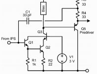
Please Bob, i am facing some troubles related the 33pf capacitor in your cascode VAS
At the first moment i have imagined the tripple darlington was the issue..then i have removed the first from the three stages, re adjusted the floating emitter resistor to 220 with the output back to EF double darlington..
I cannot reduce this capacitor below 130pF without face oscilations...with three stages at the output, with two stages and tried even with a single stage... please, confirm this value.... and....if you wish, tell a little bit more about this circuit.... i know it was made to "see" higher impedance.
I have readed your excellent book, but sadly the circuit i chose to try if driving me crazy.
I have used a very modified circuit into the Mark One...but even this way the circuit is unable to work with 33pf..... less than 130pf it starts to oscilate.... wave form becomes an amplitude modulated carrier with some few Megahertz in the carrier.
Circuit really reduces distortion but square wave form resulted very bad....not a good slew rate...raise time no good.
Is this 30pf just a reference?
Thank you,
regards,
Carlos
Attachments
Last edited:
- Home
- Amplifiers
- Solid State
- Bob Cordell's Power amplifier book