Re: NDFL, 2nd reply
Glen, just to make you curious, I have fiddled a bit with the original Alexander amp. Simulated THD20=100ppm at 50W into 8Ohms (measured: 90ppm, not bad for a sim, don't you think so).
After applying NDFL, as roughly outlined in post 2761, and keeping the ULGF of both loops at 1MHz (and equal to the original version), the THD20 drops to 10ppm.
However, as expected, the overdrive recovery is nasty.
Regards,
Edmond.
G.Kleinschmidt said:.......
I've never really looked at the Alexander amp, but when you find your files post them up, they should be interesting.
Cheers,
Glen
Glen, just to make you curious, I have fiddled a bit with the original Alexander amp. Simulated THD20=100ppm at 50W into 8Ohms (measured: 90ppm, not bad for a sim, don't you think so).
After applying NDFL, as roughly outlined in post 2761, and keeping the ULGF of both loops at 1MHz (and equal to the original version), the THD20 drops to 10ppm.
However, as expected, the overdrive recovery is nasty.
Regards,
Edmond.
Re: Re: NDFL, 2nd reply
Hi Edmond.
I've been putting any comment on hold until I had time to play with this circuit myself, but I just have not had the time. Sorry
Far too busy with other stuff, unfortunately.
Cheers,
Glen
Edmond Stuart said:
Glen, just to make you curious, I have fiddled a bit with the original Alexander amp. Simulated THD20=100ppm at 50W into 8Ohms (measured: 90ppm, not bad for a sim, don't you think so).
After applying NDFL, as roughly outlined in post 2761, and keeping the ULGF of both loops at 1MHz (and equal to the original version), the THD20 drops to 10ppm.
However, as expected, the overdrive recovery is nasty.
Regards,
Edmond.
Hi Edmond.
I've been putting any comment on hold until I had time to play with this circuit myself, but I just have not had the time. Sorry
Far too busy with other stuff, unfortunately.
Cheers,
Glen
Glen, no problem at all. Take your time.
In the meantime I try (again) to figure out how to calculate the caps and resistors.
Cheers,
Edmond.
In the meantime I try (again) to figure out how to calculate the caps and resistors.
Cheers,
Edmond.
Re: Re: NDFL, 2nd reply
Well, not any more:
Edmond Stuart said:..............
However, as expected, the overdrive recovery is nasty.
.............
Well, not any more:
Attachments
Nested clamp
(cont'ed from post 2784)
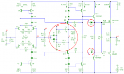
Below an example of a nested clamp applied to a very simple complementary amp. For claritity no NDFL, TMC, etc. and no optimization for lowest distortion.
The primary clamping diodes are D7 and D7. However, they are not connected in the usual way, that is, between the VAS output and base of the preceding EF stage. Instead, they are connected between emitters of aforementioned EF stage (Q9 resp. Q10) and the driver (Q13 resp. Q14). In doing so, the clamping diodes will not directly limit the VAS voltage, rather, they will create a quite large current in one of the EF stages. It is this current, tapped from the common collector node W, that is used as a feedback signal to the inverting input of the IPS. In this way, all subsequent stages will not get overloaded neither saturated. The minimum Vce of the VAS trannies is limited to 0.5V and will not depend on the output load.
I should be noted that the advantages over a conventional Baker clamp are not overwhelming in this simple amp. However, in case of NDFL for example, the clamping behavior is far better, not to say perfect (no sticking or ringing, see previous post).
A few more remarks: In order to prevent distortion, the FB current passes a threshold, comprised of D!, D2, R17 and R18. To increase HF stability also a lead lag compensation has been added: R19, R22 and C5.
And a final remark: opposed to the traditional Baker clamp, D7 and D8 itself do not contribute to additional distortion, as both sides are connected to a low impedance node (i.e. emitters).
I hope this contribution will inspire the DIY community, in particular those who are interested in NDFL amps or other topologies which are prone to bad over drive recovery.
Regards,
Edmond.
(cont'ed from post 2784)
Below an example of a nested clamp applied to a very simple complementary amp. For claritity no NDFL, TMC, etc. and no optimization for lowest distortion.
The primary clamping diodes are D7 and D7. However, they are not connected in the usual way, that is, between the VAS output and base of the preceding EF stage. Instead, they are connected between emitters of aforementioned EF stage (Q9 resp. Q10) and the driver (Q13 resp. Q14). In doing so, the clamping diodes will not directly limit the VAS voltage, rather, they will create a quite large current in one of the EF stages. It is this current, tapped from the common collector node W, that is used as a feedback signal to the inverting input of the IPS. In this way, all subsequent stages will not get overloaded neither saturated. The minimum Vce of the VAS trannies is limited to 0.5V and will not depend on the output load.
I should be noted that the advantages over a conventional Baker clamp are not overwhelming in this simple amp. However, in case of NDFL for example, the clamping behavior is far better, not to say perfect (no sticking or ringing, see previous post).
A few more remarks: In order to prevent distortion, the FB current passes a threshold, comprised of D!, D2, R17 and R18. To increase HF stability also a lead lag compensation has been added: R19, R22 and C5.
And a final remark: opposed to the traditional Baker clamp, D7 and D8 itself do not contribute to additional distortion, as both sides are connected to a low impedance node (i.e. emitters).
I hope this contribution will inspire the DIY community, in particular those who are interested in NDFL amps or other topologies which are prone to bad over drive recovery.
Regards,
Edmond.
Attachments
Edmond, quite ingenious!
One thing I wonder, is there any measurable impact on linearity? Even if the diodes are nominally 'off' they still may have enough leakage to impact the ips. Did you check this aspect?
Jan Didden
One thing I wonder, is there any measurable impact on linearity? Even if the diodes are nominally 'off' they still may have enough leakage to impact the ips. Did you check this aspect?
Jan Didden
Nested clamp
Thx.
Hi Jan,
No impact, as the AC voltages at both sides of the threshold diodes (D1 & D2) are virtually zero. R17 and R18 take care of that, as they provide a copy of the voltage at node FB (R17/R18=R11/R12=C5/C3).
Regards,
Edmond.
PS: Happily you have added Brian as well to your 'list'. He has done a lot of work on analyzing HEC and 'DEC'.
janneman said:Edmond, quite ingenious!
Thx.
One thing I wonder, is there any measurable impact on linearity? Even if the diodes are nominally 'off' they still may have enough leakage to impact the ips. Did you check this aspect?
Jan Didden
Hi Jan,
No impact, as the AC voltages at both sides of the threshold diodes (D1 & D2) are virtually zero. R17 and R18 take care of that, as they provide a copy of the voltage at node FB (R17/R18=R11/R12=C5/C3).
Regards,
Edmond.
PS: Happily you have added Brian as well to your 'list'. He has done a lot of work on analyzing HEC and 'DEC'.
Re: Nested clamp
Well yes, but with increasing Vout the voltage across the diodes also increases until they start to conduct. And that conduction point is not sharply defined, so to me it seems that there is some increasing impact before the clamping point. I don't know where exactly this is (short of measuring or simming it myself) but know from personal experience that it is very hard to avoid.
Jan Didden
Edmond Stuart said:[snip]No impact, as the AC voltages at both sides of the threshold diodes (D1 & D2) are virtually zero. R17 and R18 take care of that, as they provide a copy of the voltage at node FB (R17/R18=R11/R12=C5/C3).[snip]
Well yes, but with increasing Vout the voltage across the diodes also increases until they start to conduct. And that conduction point is not sharply defined, so to me it seems that there is some increasing impact before the clamping point. I don't know where exactly this is (short of measuring or simming it myself) but know from personal experience that it is very hard to avoid.
Jan Didden
Nested clamp
Hi Jan,
At full power and 20kHz the AC voltage across the diodes is 18mV-eff.
Whether sharply defined or not, it's still far less than the reverse voltage of say 90V pk-pk of a conventional Baker clamp diode.
In another application, with far less distortion (0.3ppm) the effect was also negligible.
Regards,
Edmond.
edit: The DC voltage across the diodes is 16mV.
nfb clamp
(second reply)
Hi Jan,
I've added one more threshold network (1 C, 2 R's and 2 D's) to make sure the diodes have absolutely no impact on distortion. Well, almost no impact: less than 1ppb.
>... but with increasing Vout the voltage across the diodes also increases until they start to conduct.....
No. Now, the voltage across the diodes is even further reduced to less than 1mV at any Vout (unless the amp is clipping, of course).
Are we on cross purposes?
Cheers,
Edmond.
janneman said:Edmond, quite ingenious!
One thing I wonder, is there any measurable impact on linearity? Even if the diodes are nominally 'off' they still may have enough leakage to impact the ips. Did you check this aspect?
Jan Didden
(second reply)
Hi Jan,
I've added one more threshold network (1 C, 2 R's and 2 D's) to make sure the diodes have absolutely no impact on distortion. Well, almost no impact: less than 1ppb.
>... but with increasing Vout the voltage across the diodes also increases until they start to conduct.....
No. Now, the voltage across the diodes is even further reduced to less than 1mV at any Vout (unless the amp is clipping, of course).
Are we on cross purposes?
Cheers,
Edmond.
Re: Nested clamp
Hi Edmond,
Very nice. I've also tried a similar closed-loop Baker clamp with the topology of my original MOSFET EC amp. When the Baker clamps in that design do their thing, the VAS current ends up being diverted through Baker clamp reference emitter followers Q18 and Q19. A portion of the signal produced if the collectors are joined and loaded to ground by a single resistor is fed back to the inverting input of the IPS. This keeps the loop closed and the IPS/VAS in a non-clipping operating mode.
In the arrangement I used, the values were such that the amplifier would tolerate an input 6 dB above overall (Baker-controlled) clipping and still keep the IPS-VAS out of clipping).
This arrangement was quite stable and prevented the minor amount of sticking in my design that Glenn had expressed concern about a few months back (that being caused by some charge buildup on the LTP collector R-C shunt network during clipping).
Cheers,
Bob
Edmond Stuart said:(cont'ed from post 2784)
Below an example of a nested clamp applied to a very simple complementary amp. For claritity no NDFL, TMC, etc. and no optimization for lowest distortion.
The primary clamping diodes are D7 and D7. However, they are not connected in the usual way, that is, between the VAS output and base of the preceding EF stage. Instead, they are connected between emitters of aforementioned EF stage (Q9 resp. Q10) and the driver (Q13 resp. Q14). In doing so, the clamping diodes will not directly limit the VAS voltage, rather, they will create a quite large current in one of the EF stages. It is this current, tapped from the common collector node W, that is used as a feedback signal to the inverting input of the IPS. In this way, all subsequent stages will not get overloaded neither saturated. The minimum Vce of the VAS trannies is limited to 0.5V and will not depend on the output load.
I should be noted that the advantages over a conventional Baker clamp are not overwhelming in this simple amp. However, in case of NDFL for example, the clamping behavior is far better, not to say perfect (no sticking or ringing, see previous post).
A few more remarks: In order to prevent distortion, the FB current passes a threshold, comprised of D!, D2, R17 and R18. To increase HF stability also a lead lag compensation has been added: R19, R22 and C5.
And a final remark: opposed to the traditional Baker clamp, D7 and D8 itself do not contribute to additional distortion, as both sides are connected to a low impedance node (i.e. emitters).
I hope this contribution will inspire the DIY community, in particular those who are interested in NDFL amps or other topologies which are prone to bad over drive recovery.
Regards,
Edmond.
Hi Edmond,
Very nice. I've also tried a similar closed-loop Baker clamp with the topology of my original MOSFET EC amp. When the Baker clamps in that design do their thing, the VAS current ends up being diverted through Baker clamp reference emitter followers Q18 and Q19. A portion of the signal produced if the collectors are joined and loaded to ground by a single resistor is fed back to the inverting input of the IPS. This keeps the loop closed and the IPS/VAS in a non-clipping operating mode.
In the arrangement I used, the values were such that the amplifier would tolerate an input 6 dB above overall (Baker-controlled) clipping and still keep the IPS-VAS out of clipping).
This arrangement was quite stable and prevented the minor amount of sticking in my design that Glenn had expressed concern about a few months back (that being caused by some charge buildup on the LTP collector R-C shunt network during clipping).
Cheers,
Bob
Re: nfb clamp
No, not at all. I appears you have effectively got your cake and are eating it too 😉
Jan Didden
Edmond Stuart said:[snip]Are we on cross purposes?
Cheers,
Edmond.
No, not at all. I appears you have effectively got your cake and are eating it too 😉
Jan Didden
Re: Re: Nested clamp
Thanks Bob.
Using your words, great minds think alike. However, there's one caveat: loop stability!
Cheers,
Edmond.
Bob Cordell said:Hi Edmond,
Very nice. I've also tried a similar closed-loop Baker clamp with the topology of my original MOSFET EC amp. When the Baker clamps in that design do their thing, the VAS current ends up being diverted through Baker clamp reference emitter followers Q18 and Q19.
[snip]
Cheers,
Bob
Thanks Bob.
Using your words, great minds think alike. However, there's one caveat: loop stability!
Cheers,
Edmond.
Hi Edmond,
I saw your circuit a while back, but wasn't sure how to incorporate it into a Blameless topology. Then I saw Glen's post here and just went "duh!". I played around with it a bit, and found some ringing on the initial clip. I could almost eliminate the ringing by increasing the capacitor in the series RC compensation network, but then the distortion increased. Then I noticed his network didn't use one of the resistors in your lag-lead network. I went back to your network and just impedance scaled it (since it appears we're using the same gain), and was able to get very low overshoot and ringing on initial clipping as well as negligible impact on distortion - the best of both worlds. I still get about 0.7 Volts overshoot on an 85V peak output though, but the clipping behavior is so much better than before (using a clamp without feedback) that I'm still quite happy with it.
Were you able to analytically determine the compensation values somehow, or were they determined experimentally?
Another thing I was worried about was the resistor ratio matching between the clipping and feedback networks. With 80V peak out and 1 percent mismatch in resistor ratios, this would turn on the diodes that go back to the inverting input. So I decided to use the same values for the feedback and clipping dividers and use two series diodes each in these spots just to be safe. This way I can match up the resistors if I want to. It's probably unnecessary though.
Since my design uses a boosted front end supply for everything except the output FETs themselves, I want to try basing the clipping on the Vgd of the output FETs and having the drivers provide the current for the clipping network instead of the VAS. Still, with good diodes like the BAV21, the distortion increase in simulation with these diodes at the VAS output is negligible. I have a protection circuit that clamps the VAS output to zero, so unfortunately I'm still stuck with diodes there.
andy_c said:Hi Edmond,
I saw your circuit a while back, but wasn't sure how to incorporate it into a Blameless topology. Then I saw Glen's post here and just went "duh!". I played around with it a bit, and found some ringing on the initial clip. I could almost eliminate the ringing by increasing the capacitor in the series RC compensation network, but then the distortion increased. Then I noticed his network didn't use one of the resistors in your lag-lead network.
Hi Andy
As can be seen in that post of mine, the clipping for the whole amp was perfect with zero ringing. I've since deleted that sim file but I don't recall that the compensation cap was overly large.
The feedback bit of the clamp didn't add any extra distortion that I could see.
What type of compensation are you using for the whole amplifier?
Is it the PSRR mod that returns the Miller cap to an LTP cascode emitter? That would require an extra R-C on the LTP output to stabilise the Miller loop (not shown in D.Self's book!), which causes sticking unless a feedback clamp is used.
Cheer,
Glen
G.Kleinschmidt said:As can be seen in that post of mine, the clipping for the whole amp was perfect with zero ringing. I've since deleted that sim file but I don't recall that the compensation cap was overly large.
The feedback bit of the clamp didn't add any extra distortion that I could see.
What type of compensation are you using for the whole amplifier?
Is it the PSRR mod that returns the Miller cap to an LTP cascode emitter? That would require an extra R-C on the LTP output to stabilise the Miller loop (not shown in D.Self's book!), which causes sticking unless a feedback clamp is used.
That's exactly right - the PSRR mod. Sticking was godawful with a normal clamp and did indeed require the feedback clamp to avoid that mess. Compensation of the Miller loop was with a series RC at the current mirror output, giving the Miller loop about a 10 MHz ULG freq. This compensatin technique seems to work fine, as this is a very high impedance point. But the sticking of this circuit is nasty. I suspect the difference between what you and I saw is due to my use of that technique, just as you mentioned. At any rate, that additional resistor in the clamp compensation seems to give more flexibility in stabilizing the feedback clamp and worked well for me.
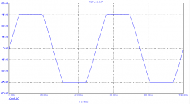
Edit: Found a partial pic of the circuit. It's in this post
Edit 2: The other difference is that I'm biasing the clamp EF in cutoff like in VSOP. I'll look to see if that is affecting the overshoot.
Edit 3: I'm visiting relatives, so I can only pop in from time to time 🙂.
NFB clamp
Hi Andy,
So now we are both happy. 😀
Not analytically. There are too many variables involved. I just simmed it.
If you use the same ratio for the feedback and clipping dividers, the only thing that matters is the input voltage, not that huge output voltage.
You can eliminate the adverse effect of those protection diodes. I'll send you the schematic. Perhaps you might use it as well.
Cheers,
Edmond.
andy_c said:Hi Edmond,
I saw your circuit a while back, but wasn't sure how to incorporate it into a Blameless topology. Then I saw Glen's post here and just went "duh!". I played around with it a bit, and found some ringing on the initial clip. I could almost eliminate the ringing by increasing the capacitor in the series RC compensation network, but then the distortion increased. Then I noticed his network didn't use one of the resistors in your lag-lead network. I went back to your network and just impedance scaled it (since it appears we're using the same gain), and was able to get very low overshoot and ringing on initial clipping as well as negligible impact on distortion - the best of both worlds. I still get about 0.7 Volts overshoot on an 85V peak output though, but the clipping behavior is so much better than before (using a clamp without feedback) that I'm still quite happy with it.
Hi Andy,
So now we are both happy. 😀
Were you able to analytically determine the compensation values somehow, or were they determined experimentally?
Not analytically. There are too many variables involved. I just simmed it.
Another thing I was worried about was the resistor ratio matching between the clipping and feedback networks. With 80V peak out and 1 percent mismatch in resistor ratios, this would turn on the diodes that go back to the inverting input. So I decided to use the same values for the feedback and clipping dividers and use two series diodes each in these spots just to be safe. This way I can match up the resistors if I want to. It's probably unnecessary though.
If you use the same ratio for the feedback and clipping dividers, the only thing that matters is the input voltage, not that huge output voltage.
Since my design uses a boosted front end supply for everything except the output FETs themselves, I want to try basing the clipping on the Vgd of the output FETs and having the drivers provide the current for the clipping network instead of the VAS. Still, with good diodes like the BAV21, the distortion increase in simulation with these diodes at the VAS output is negligible. I have a protection circuit that clamps the VAS output to zero, so unfortunately I'm still stuck with diodes there.
You can eliminate the adverse effect of those protection diodes. I'll send you the schematic. Perhaps you might use it as well.
Cheers,
Edmond.
- Home
- Amplifiers
- Solid State
- Bob Cordell Interview: Negative Feedback