traderbam said:Andy, Ive run a few sims on the circuit you posted. I notice that there is a negative feedback loop of G1, E1, R5 such that the loop gain from the output appears to be close to unity...no apparent feedback from the output. I may have got something wrong.
You are right that it's a kind of feedback. The product of the voltage divider ratio of R5-R6-R12 and the diff amp gain must have a magnitude of exactly one and the correct sign to get the theoretical cancellation of the error. The capacitor C1 prevents this from occurring exactly, which is why I suggested taking it out as an experiment to show that complete error cancellation (within the LTSpice residual error) occurs.
It's also possible to get the theoretical cancellation with R12 = infinity. In this case the error correction is trying to set the gain of the circuit to exactly 1 out to infinite frequency (assuming C1 has been removed). Part of the error is that the gain of the MOSFET follower is something like 0.95 rather than 1. If you look at the voltage drop across the error correction resistors R1 and R2 in the transient analysis, you'll see that when R12 is infinity, the error correction signal consists almost entirely of the fundamental. That is, it's mostly a gain correction. When the output voltage becomes large, this fundamental component starts to use up more and more of the available dynamic range of the error correction. To correct this, I chose the R5-R6-R12 divider ratio to equal the simulated small-signal "gain" of the MOSFET follower. To make it so the error correction still had ideal cancellation, this required adjusting the diff amp gain. This results in a slightly different block diagram from Bob's Figure 11. With Rsh set to the value of my original post, the error correction signal consists almost entirely of distortion. This maximizes the available dynamic range of the error correction. If you wish to adjust R12, do so by editing the Rsh .PARAM statement rather than the resistor value itself. This will automatically adjust the diff amp gain. Note that when many output devices are paralleled, the gain of the MOSFET follower approaches 1 and the benefits of Rsh become negligible.
Although it's a feedback circuit, it's not a high loop gain feedback circuit. If you wish to quantify the loop gain (in the Middlebrook sense), you can use the attached loop gain probe, courtesy of Frank Weidemann (sp?) of the LTSpice user's group. If you wish to do so, the directions are in the LoopGain_Probe.asc. I found it helpful in that file to right-click on the blue comment text, locate the loop gain formula and copy it to the clipboard from there. You'll also need to set up the .STEP directive as in the example, name the probe Xlp, and pass the lpvar parameter from the lp parameter as the example does. If you run that sim, you'll see the loop gain is very low at low frequencies, but as the output stage rolls off, it can have a magnitude greater than one. Of course, the phase becomes critical in this case. You can observe the effects of C1 on this.
Attachments
andy_c said:.......it's not a high loop gain feedback circuit..........
This is true, and is readily seen by noting that it is series derived negative feedback amplified by a single transistor (viz. stylized as summer S1) .
This further suggests that compensation need not be too rigorous.
That's curious, Andy. I measure the loop gain to be 84dB at 1kHz and unity at 16MHz, with a 200pF compensation cap. I'll check out that probe method. What unity gain f do you get?
Some of the loop gain methods have inaccuracies that depend on the circuit impedances. The loop gain probe of that attachment can be put anywhere inside the loop with correct results.
Also, be sure to set the AC value of V5 to zero.
Also, be sure to set the AC value of V5 to zero.
Andy,
I was already using the Middlebrook method without realising it. I'm talking about the loop that contains the connection between output and G1/G2.
I'm pretty sure you'll find the same. The rather high distortion of the FETs can only be reduced to near zero by enormous amounts of feedback. The loop gain is generated by the positive feedback loop between G1 and E1 and is rolled off by the Cgs of the FET.
The only reason you need C1 to make this idealised model stable is because of R8 and R9 adding a pole in the forward loop. If you make them zero and C1 zero you'll have a stable system with 40 deg of phase margin with pole 2 at about 100MHz. Alternatively, leave R8 and R9 as is and increase Rsh to reduce the forward path gain and achieve stability with C1 = 0.
Brian
traderbam said:The rather high distortion of the FETs can only be reduced to near zero by enormous amounts of feedback.
Hi Brian,
Since the loop gain is a property of the linearized network, distortion should not enter the picture. If I've done my homework correctly, the voltage divider will have the same voltage "gain" as the FETs. Assume for the sake of argument that the FETs have infinite bandwidth. Without C1, and with infinite bandwidth FETs, the voltages at the input of the diff amp will be equal over all frequencies, because I've made the attenuation of the voltage divider the same as the FETs. This means the AC component of the error correction currents at the diff amp output will be zero (assuming the attenuations are exactly equal). This means that the loop gain would be zero. I'm sure there's some numerical error in the resistor values that makes this inexact though.
Later today I'll try to post a version of the circuit with the loop gain probe in place. I'm tied up at the moment, so it may be late for you. It's possible that we're talking about two different thngs.
Andy
Take as long as you like to reply. 🙂
I understand what you are describing and I agree with all of it.
I understand what you are describing and I agree with all of it.
Quite interesting thread! I agree that the error correction concept in a sense is positive feedback leading to infinite loop gain. Intuitively that can be seen if one realises that the EC circuit bootstraps its own input signal. But the difference with other schemes - and it is a crucial one - is that this pertains only to the error signal.
Someone, I think it was Traderbam and/or Mikeks noted that less compensation was needed. I think the reason for that is that although the system might have a high loop gain, the fundamental is subtracted from the output signal before the result is fed back to that self-bootstrapping input. So, the apparent high loop gain (by the pos feedback) is divided by the cancellation ratio of Vout and Vin (of the amp) in the subtractor.
If you work with these circuits it is really very apparent. Whereas 'normal' fb circuits are unforgiving if you don't get the compensation right (and we all know that is no easy task on the test bench with a spiderweb wiring), EC is lame in comparison. Just a little EC loop roll-off to tame it.
I think the crucial difference with other null-networks is indeed the cancellation of the fundamental before you close that loop. And I have a hunch that Hawksford realised that when he limited his application to a system that had close to unity gain. In theory, it works also with gain blocks that have gains significantly differing from unity, but there the fundamental cancellation is less large, the fundamental enters the loop and the system is less stable.
Jan Didden
janneman said:I agree that the error correction concept in a sense is positive feedback leading to infinite loop gain.
Jan Didden
Not sure about this; care to explain?

Hi Jan,
Good exercise for the brain, eh? 🙂
I think the ease of stability you mention is because in this case the overall gain from preceding stage to output is 1 or less, and the bandwidth is extended.
But within the EC circuit itself, I believe there is a barely tamed animal! Just like an op-amp in unity gain, non-inverting configuration. There is a huge amount of feedback due to the bootstrapping.
Try calculating the OL gain of the circuit by looking at the schematic. Disconnect the feedback signal from the output. What will the gain be? We know that the feedback factor is the ratio of OL to CL gain, so what does the feedback factor look like?
Another approach is to think about how the circuit can possibly correct an error without using feedback. What it attempts to do is to subtract input from output and feed it back into the input. But we know that for a non-linear function the subtractive error cannot possibly be the conjugate function needed to produce an error-free output. So the system has no choice but to "hunt" for an equilibrium solution.
Consider the equations in Hawkford's paper. The eq(1) is always correct. But he then assumes an equality, b = (1-a), to simplify the eq(1) to make eq(3) Vout = Vin. This sets a trap for the circuit implementor! When b=0, (1-a)=0 and eq(1) then contains singularities:
Vout = N(Vn) { 1 - 0/0 } + 0/0 Vin
In algebra, these tend to 1 "in the limit" (and is instantaneously equal to 1). Like magic. But the real circuit wasn't taught algebra at school so it must "hunt" for the equilibrium solution. If we are lucky it finds it rather than oscillates.
That's my theory, anyhow. 😉
Brian
Not sure about this folks: looking at fig. 11, it would appear that the algebraic sum of the error signal ''e'' and the input ''x'' drives the output stage.
In other words, this is negative feedback applied to the output stage's input. Loop gain cannot be very high since it is largely generated by a single transistor.
In other words, this is negative feedback applied to the output stage's input. Loop gain cannot be very high since it is largely generated by a single transistor.
Hi all,
Wow, I was getting some very high loop gain numbers too. I started to question my own sanity. After all, if the attenuations of the voltage divider and MOSFETs are nearly the same (as they are by design), the error signal at the diff amp output should almost cancel, giving a very low loop gain.
Then I realized that there's really two feedback paths - one from the divder and one from the MOSFET output. Unless the loop gain probe is in the innermost loop, some strange results will happen. So I moved the loop gain probe so it's in the innermost loop and got the expected results.
Attached are the project and support files. Graph will be in next post.
Attachments
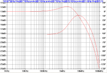
Okay, here is the plot of loop gain. The upper plot is the phase and the lower plot is the magnitude. You can repeat this yourself with the previously posted project by editing the comment field with the loop gain expression and copying the loop gain formula into the output expression for the plot.
You can see at low frequencies that the loop gain is a little less than -18 dB in magnitude. I think this could be made much lower by better matching of the voltage divider ratio to the small-signal MOSFET gain.
You can see at low frequencies that the loop gain is a little less than -18 dB in magnitude. I think this could be made much lower by better matching of the voltage divider ratio to the small-signal MOSFET gain.
Attachments
Oh yes. In the loop gain example I posted a while back, one of the instructions is to go into the LTSpice control panel "Save Defaults" tab and check "save device currents", "save subcircuit node voltages" and "save subcircuit device currents". This results in very big .raw files being left behind, so in the "Operation" tab I set "Automatically delete .raw files" to yes.
I think the problem is that subcircuit voltages and/or currents are being referred to in the loop gain expression but they are not being saved in the .raw file.
Does this fix it Mike?
I think the problem is that subcircuit voltages and/or currents are being referred to in the loop gain expression but they are not being saved in the .raw file.
Does this fix it Mike?
mikeks said:
Not sure about this; care to explain?
You should hve left the next scentence in the quote 😉
I mean that as the ec circuit bootstraps its own input, that's pos fb, no?
Jan Didden
andy_c said:[snip]You can see at low frequencies that the loop gain is a little less than -18 dB in magnitude. I think this could be made much lower by better matching of the voltage divider ratio to the small-signal MOSFET gain.
If the divider ratio and forward gain match exactly, the loop gain for the main signal (carrier?) goes to zero. That's what I meant by saying that the apparent huge loop gain (due to pos fb) is divided by the cancellation ratio. My experience is that the closer the forward gain is to the ec return gain, the more stable the circuit is.
Jan Didden
Wow, I was getting some very high loop gain numbers too. I started to question my own sanity.

Then I realized that there's really two feedback paths - one from the divder and one from the MOSFET output. Unless the loop gain probe is in the innermost loop, some strange results will happen. So I moved the loop gain probe so it's in the innermost loop and got the expected results.

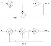
Try this. Fig.1 is the Hawksford/BC system. Fig. 2 is the exact same system drawn in a different way. The two are equivalent. That "strange result" you see is not strange at all...your sanity is not in question. You were measuring the loop gain in path D. This is the path that includes the output device - the device that we are trying to "correct".
Attachments
- Home
- Amplifiers
- Solid State
- Bob Cordell Interview: Error Correction