HF voltage drop on probe or measuring cable shield impedance. Various mechanism of interference coupling. Years behind the scope screen 😉 , solving instruments for high EMI environment, like HV Labs and power testing labs.
Re: Re: Re: Re: "Naked base-emitter junctions"?
But I have.
Your turn now.
Regards,
Milan
mikeks said:.. try it...
[/B]
But I have.
Your turn now.
Regards,
Milan
Attachments
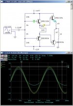
Actually, you haven't; doesn't even look remotely like locanthi's circuit 🙄
Try again; use this circuit.
Try again; use this circuit.
Now, look what you made me do, mikeks! Don't you think it's about time you start doing your homework yourself? You can wiggle all you want now... or just make your own sims.
Regards,
Milan
You can wiggle all you want now... or just make your own sims. Regards,
Milan

Driver transistors operate in Class A
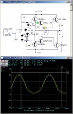
Referring to the actual circuit being discussed, posted most recently in Post #173, we can see without simulation why the driver transistors Q7, Q8 remain in Class A even when the output transistors are in Class B. Although I am an advocate of simulation, this question can be answered quickly with pencil and paper by postulating a simple scenario.
Assume that the amplifier output voltage is at +16V, and delivering 2A into an 8-ohm load to ground. Now work your way backward through the conducting path comprising the upper set of transistors. R12 will drop about 0.7V, putting the emitter of Q9 at +16.7. Its base will then be at +17.4. Q7's base will then be at about +18.0. Q5's base will be at about +18.6. The bias network needed all along to have a fixed drop of about 4.0V. This means that the base of Q6 must be at about +14.6.
We now work our way forward through the bottom set of transistors. Q6 will be off with a reverse base-emitter bias of about 1.4V, since both ends of R10 are sitting at the output voltage level of +16.0. The base of Q8 is therefore at about +16.0 also (ignoring insignificant base current). Since Q8's emitter resistor R11 is set at its far end to +17.4V (at the emitter of Q7), Q8 is turned on, with its emitter sitting at about +16.6V. The drop across R11 is thus about 0.8V, and R11, at 56 ohms, will be conducting about 14 mA. Output transistor Q10 will be off with a reverse base-emitter bias of about 0.6V. Thus, Q7 and Q8 are both conducting current and operating in Class A, while output transistors Q9 and Q10 are in Class B, since only Q9 is active.
As an interesting exercise, disconnect the junction of R9 and R10 from the output node, so this pair of resistors becomes a single 660 ohm resistor, and we get the classic Locanthi "T" circuit. Now re-do the analysis and see what you see. I do not mean to imply that one way is better than the other, just different.
Finally, please all keep in mind that this circuit was not published by me as an example of a really good amplifier - it was just used in one of my papers as an example of a typical bipolar amplifier of the time (back in the late '70's).
Bob Cordell
Give SPICE a try
In an earlier post Wavebourn indicated that he essentially simulates his circuits in his head and does not use SPICE. In fact many of the best designers are very adept at doing just this in the course of designing a circuit. Indeed, I must admit that back in 1981 when I did my MOSFET power amplifier with error correction, I did little or no SPICE simulation on it. At the time, SPICE pretty much only ran in batch mode on Unix systems, and did not have a very friendly interface.
However, a lot has changed in the last 25 years, with excellent versions of SPICE with good human interfaces available for free that will run on any decent PC. This is one of the least expensive things you can add to your arsenal of tools for designing amplifiers. As an analysis tool, SPICE is not a replacement for the intuitive, interactive design sysnthesis process that goes on in the head of a good designer, but it can let you see things you might never have seen, and allow you to gain insight from quick and easy experiments you can perform in the simulation domain.
There is an especially nice free version of SPICE out there that I use, made available by Linear Technology, maker of some very good op amps and other ICs. Go to www.linear.com. Click on Design Support. Click on Design Simulation. Click on LTSpice/SWCADIII. Download this version of SPICE and have fun. You'll get hooked.
One caveat, as with any computer tool, garbage-in, garbage-out. SPICE simulation is not a replacement for common sense and mental sanity checks.
Cheers,
Bob Cordell
Thank you Bob! I am not a Mammoth, and I am not against indeed very convenient and smart tools... I just wanted to say that their availability and convenience don't teach modern engineers to think...
I too tend to "simulate in my head", always have as it's the main part of intuitive design IMHO, but I certainly can't hear the amplifier in my head before building it as Wavebourn claims to 😀
As to it being down to experiance.....I started aged 5 and I am now 41. I had read every book on electronics in every library within about 15 miles by the age of 15 or so, I have worked as a techician and later engineer on both civilian and military projects and was once chief engineer with a fairly well known hifi manufacturer....still can't hear amps in my head without building them though Wavebourn 😉 How much experiance do I need?
Spice can be a wonderful tool for fairly "tame" circuitry but foolish is the man who does not breadboard any high gain and bandwidth/high frequency circuit as the "sproggies" will get ya every time 😉
OK guys, shall we get back to error correction amps? It is a great opportunity to have Bob in here, and there are several of us who has made experience with designing of this kind of amps.
PMA said:OK guys, shall we get back to error correction amps? It is a great opportunity to have Bob in here, and there are several of us who has made experience with designing of this kind of amps.
Me first
Bob,
have you ever tried feedback error correction applied globally, on the whole amplifier with voltage gain? If so, what is your experience with stability?
best regards
Adam
Amplifier EMI Ingress Immunity
Here are some further thoughts on the earlier subject in the thread of EMI ingress. Much was said about how much EMI ingress there is, how and where it gets in, and how to prevent it from getting in.
The other half of the problem is the degree of the amplifier's EMI immunity, and there was some recognition that different circuit designs may have more inherent immunity than others.
Here is an idea for measuring an amplifier's EMI immunity. It has its roots in the Multitone Intermodulation (MIM) test I developed in the early '80's. In that test, we used three equal tones at 9.00, 10.05 and 20.00 kHz as a stimulous and then looked for second and third order intermodulation products at 1050 Hz and 950 Hz. These IM products were a decade below the test tone frequencies so they were easy to see with low-cost inctrumentation. (The paper describing the MIM test is posted at www.cordellaudio.com - my apologies for the poor quality of the PDF scan - I'll fix it this weekend).
Let us now use three equal tones at 990 kHz, 1001 kHz and 2000 kHz and look for IM products at 9 kHz and 11 kHz in an analogous way in the amplifier under test.
Note that the test tones are at a frequency somewhat above the gain-crossover frequency of most power amplifiers. One could, of course, apply a constellation of tones at a higher set of frequencies as well.
Note also that the IM products lie in the upper audio band near 10 khz, where there may not be as much negative feedback available to reduce them in some designs.
The three-tone HF MIM test signal can be applied in numerous ways to the amplifier, while looking for the IM products at the amplifier's output terminals. First, the tones can be applied conventionally to the input of the amplifier, at, say, a 100 mV p-p level. This could turn out to be a tough test for some amplifiers 🙂.
Secondly, the tones can be applied to the output of the amplifier through a resistance so as to create a current on the order of 10 mA p-p to 100 mA p-p. This will exercise the output stage nonlinearity in the Class-AB bias region. (I already do a version of this latter test on amplifiers using the CCIF 19 kHz + 20 khz tones and a spectrum analyzer as a very good test for crossover distortion).
Finally, the HF MIM test tone constellation can be applied to the amplifier via its power cord in either differential or common mode by inserting an appropriate (small, low-cost) HF transformer in the a.c. mains path. Here I would probably apply between 1 V p-p and 10 V p-p on the mains line, again looking for 9 kHz and 11 kHz IM products at the output of the amplifier.
Let me know what you think of this proposal for an amplifier EMI immunity test.
Bob Cordell
Global feedback error correction
Adam,
No, I have never tried feedback error correction globally. I imagine that stability would be a problem. Also, I think the output stage is really where it is needed most. We tend to be able to make Class-A input, VAS and driver circuits almost arbitrarily linear with good circuit design and conventional linearization approaches.
Best regards,
Bob
Hi Bob:
I'd like to express my doubts as to the efficiency of the MIM test with HF signals. The frequencies of the proposed HF signals are outside the DUT operational frequency range so we can't tell exactly what the attenuation (or amplification) of individual test signals is. On the other hand, in case of IM testing with the signals that are within the DUT operational range, IM products have the same statistic probability of occurring.
I'm thinking it might be better to use AM or FM narrow-bandwidth signals. In that case, the levels of demodulation products within the DUT range might be taken as an indicator of EMI immunity.
In any case, it may be a good idea to formulate some sort of a hypothesis about expected defects in the DUT due to EMI ingression (in terms of, for instance, AM demodulation, instability/self-oscillation, IM with a useful audio signal, etc.), which would then make the modeling of the optimal test signal content much easier, I believe.
Regards,
Milan
SY said:W, if you want to start a separate thread on the merits and demerits of simulation, feel free. Otherwise, let's keep this on topic.
SY, the speach was about Bob's amp where driver worked in Class A mode. And why some of us did not believe that it is true because somebody else told thst it can naver be true...
It is just in the topic.
Speaking of RF. Bob, why do you need 3 frequencies, why 2 is not enough?
Superbly intuitive analysis!
Hi Bob,
Thanks for this most illuminating analysis.
It may be inferred from the later that my assertion here was incorrect.
It is, in fact, abundantly clear now that, regardless of load, and irrespective of the fact that Q6/Q10 are turned off for positive voltage swings in Class B, device Q8 must, of necessity, be turned on by Q7 pulling its emitter high, courtesy of R11. Resplendent!
(Clearly my ebullience at discovering your membership of the forum was well justified.)
Your analysis could be further extended to demonstrate that my first assessment was correct in fact.
Indeed, cross-coupling the emitters of Q5/Q6 similarly causes Q5 to pull Q6's emitter high for positive output voltage swings, thereby driving Q6 into conduction.
Thus, causing the first pair of drivers (Q5/Q6) to conduct throughout the cycle, more effectively (and with superior linearity), isolates the second stage from the non-linear loading of the class B (or AB) output stage; the dedicated class-A emitter
follower recommended by D. Self for this purpose is made redundant.
This attribute is notably absent in this circuit, and is one of the greatest advantages of Locanthi's arrangement.
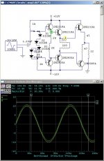
Bob Cordell said:Referring to the actual circuit being discussed, posted most recently in Post #173, we can see without simulation why the driver transistors Q7, Q8 remain in Class A even when the output transistors are in Class B. Although I am an advocate of simulation, this question can be answered quickly with pencil and paper by postulating a simple scenario.
Assume that the amplifier output voltage is at +16V, and delivering 2A into an 8-ohm load to ground. Now work your way backward through the conducting path comprising the upper set of transistors. R12 will drop about 0.7V, putting the emitter of Q9 at +16.7. Its base will then be at +17.4. Q7's base will then be at about +18.0. Q5's base will be at about +18.6. The bias network needed all along to have a fixed drop of about 4.0V. This means that the base of Q6 must be at about +14.6.
We now work our way forward through the bottom set of transistors. Q6 will be off with a reverse base-emitter bias of about 1.4V, since both ends of R10 are sitting at the output voltage level of +16.0. The base of Q8 is therefore at about +16.0 also (ignoring insignificant base current). Since Q8's emitter resistor R11 is set at its far end to +17.4V (at the emitter of Q7), Q8 is turned on, with its emitter sitting at about +16.6V. The drop across R11 is thus about 0.8V, and R11, at 56 ohms, will be conducting about 14 mA. Output transistor Q10 will be off with a reverse base-emitter bias of about 0.6V. Thus, Q7 and Q8 are both conducting current and operating in Class A, while output transistors Q9 and Q10 are in Class B, since only Q9 is active.
As an interesting exercise, disconnect the junction of R9 and R10 from the output node, so this pair of resistors becomes a single 660 ohm resistor, and we get the classic Locanthi "T" circuit. Now re-do the analysis and see what you see. I do not mean to imply that one way is better than the other, just different.
Finally, please all keep in mind that this circuit was not published by me as an example of a really good amplifier - it was just used in one of my papers as an example of a typical bipolar amplifier of the time (back in the late '70's).
Bob Cordell
Hi Bob,
Thanks for this most illuminating analysis.
It may be inferred from the later that my assertion here was incorrect.
It is, in fact, abundantly clear now that, regardless of load, and irrespective of the fact that Q6/Q10 are turned off for positive voltage swings in Class B, device Q8 must, of necessity, be turned on by Q7 pulling its emitter high, courtesy of R11. Resplendent!
(Clearly my ebullience at discovering your membership of the forum was well justified.)
Your analysis could be further extended to demonstrate that my first assessment was correct in fact.
Indeed, cross-coupling the emitters of Q5/Q6 similarly causes Q5 to pull Q6's emitter high for positive output voltage swings, thereby driving Q6 into conduction.
Thus, causing the first pair of drivers (Q5/Q6) to conduct throughout the cycle, more effectively (and with superior linearity), isolates the second stage from the non-linear loading of the class B (or AB) output stage; the dedicated class-A emitter
follower recommended by D. Self for this purpose is made redundant.
This attribute is notably absent in this circuit, and is one of the greatest advantages of Locanthi's arrangement.

Re: Superbly intuitive analysis!
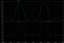
Finally, proof of the exceedingly good pudding...(4ohm load assumed)
The top plot shows Q7's collector current (green trace) with respect to this arrangement.
The navy trace represents Q7's collector current wth Q5/Q6 cross-coupled.
Similarly, the bottom plot shows Q5's collector current (red trace) with this arrangement.
The sky blue trace represents Q5's collector current wth Q5/Q6 cross-coupled.
Note that in both arrangements Q7/Q8 will operate in class A only if the output stage is at least biased in ''optimal'' class B.
mikeks said:
Hi Bob,
Thanks for this most illuminating analysis.
It may be inferred from the later that my assertion here was incorrect.
It is, in fact, abundantly clear now that, regardless of load, and irrespective of the fact that Q6/Q10 are turned off for positive voltage swings in Class B, device Q8 must, of necessity, be turned on by Q7 pulling its emitter high, courtesy of R11. Resplendent!
(Clearly my ebullience at discovering your membership of the forum was well justified.)
Your analysis could be further extended to demonstrate that my first assessment was correct in fact.
Indeed, cross-coupling the emitters of Q5/Q6 similarly causes Q5 to pull Q6's emitter high for positive output voltage swings, thereby driving Q6 into conduction.
Thus, causing the first pair of drivers (Q5/Q6) to conduct throughout the cycle, more effectively (and with superior linearity), isolates the second stage from the non-linear loading of the class B (or AB) output stage; the dedicated class-A emitter
follower recommended by D. Self for this purpose is made redundant.
This attribute is notably absent in this circuit, and is one of the greatest advantages of Locanthi's arrangement.
Finally, proof of the exceedingly good pudding...(4ohm load assumed)
The top plot shows Q7's collector current (green trace) with respect to this arrangement.
The navy trace represents Q7's collector current wth Q5/Q6 cross-coupled.
Similarly, the bottom plot shows Q5's collector current (red trace) with this arrangement.
The sky blue trace represents Q5's collector current wth Q5/Q6 cross-coupled.
Note that in both arrangements Q7/Q8 will operate in class A only if the output stage is at least biased in ''optimal'' class B.
Attachments
- Home
- Amplifiers
- Solid State
- Bob Cordell Interview: Error Correction