Similarly, loop-transmission may be determined in the Cordell output stage by first ensuring that the selected test point breaks all conceivable intra-circuit loops.
Plot the following expression
-1/(1-1/(2*(I(Vi1)@1*V(x)@2-V(x)@1*I(Vi1)@2)+V(x)@1+I(Vi1)@2))
Plot the following expression
-1/(1-1/(2*(I(Vi1)@1*V(x)@2-V(x)@1*I(Vi1)@2)+V(x)@1+I(Vi1)@2))
Attachments
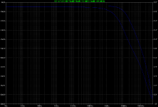
The result below (loop-gain less than unity) proves the correctness of the simpler approach above, and the correctness of this analysis.
Attachments
janneman said:
Yes you are right, in the sense that I think the common thing in the distortion of my amp is in the way the summers are implemented. They are the same in the Vas and the power stage so both show similar distortion characteristics. I hope that when I improve the summer(s) the whole thing improves, but I have no real ideas so far.
You are also correct that it looks not particularly better or worse then 'normal' global nfb amps. It was not my intend to improve on that, but trying to get to the same quality level without global nfb, and my results show it is possible. Of course I can try to further improve by applying extra loop gain and global nfb, but for the time being I like to see if I can improve the amp in its current topology and then publish it.
Jan Didden
Hmm, when I was a bit more convinced that the Hawksford EC
would give better results then NFB I would try it for myself......😉
Heinz
@powerbecker adn gootee: how times do you spend to have result of simualtion ? I don't know why LTSpice runs too slowly with your schematic. Actually I never finished simulate your schematic
Bye!
Bye!
thanh said:@powerbecker adn gootee: how times do you spend to have result of simualtion ? I don't know why LTSpice runs too slowly with your schematic. Actually I never finished simulate your schematic
Bye!
Not so long : 6.142 sec, use the Alternate Solver !
Heinz!
Attachments
traderbam said:I was looking at PFB distortion vs integrator distortion last night. I made two spice models, each using two BJTs. The PFB was like Bob's darlington. The integrator was made using a capacitor, NFB loop. The BJTs were run at identical bias currents, I made the frequency responses as close as I could, etc. I found in the PFB the distortion of the BJTs was amplified, the output Z was increased and the input Z increased. The opposite with the NFB integrator. Consider that the circuit is being fed from a fairly low Z and is driving non-linear FET input Z.
Did you see my questions about those Spice models, Andy?
I did not see these questions Brian. I am starting to get caught up in family holiday issues, so I can only post sporadically at the moment. Maybe if you could email me I could clear this up or at least find out what it's all about?
powerbecker said:
Hmm, when I was a bit more convinced that the Hawksford EC
would give better results then NFB I would try it for myself......😉
Heinz
Well, in electronics like in real life, brute force often has the edge 😉 . But playing with ec is quite interesting. Notwithstanding the discussions here that it is equivalent to nfb, the character, if I can call it that, of an ec amp is definitely different from a nfb amp.
You really have to think differently, there is no longer the overriding concern to get very high gain. What strikes me is the almost complete adsense of oscillatory tendencies, ec circuits (at least in my experience) tend to be very docile.
If you are looking to something different from the tired old ways, ec amps are worth a try!
Jan Didden
mikeks said:The result below (loop-gain less than unity) proves the correctness of the simpler approach above, and the correctness of this analysis.
Mike I hope I get some time this weekend to look at your analysis. I agree that the 'actual' ec loop gain is somehow proportional to the extracted error but hadn't realised the equation was so neat.
Nice work, thanks!
Jan Didden
Hi Mikes, re Post #1338:
1st circuit "loop gain" test with unity gain output seems to demonstrate that you made a pretty hi cmrr diff amp with U2
more informative to my mind is moving R9_1 ( “inverting input” of U2 viewed as a diff amp) left of the test source V1, this tests the loop gain the “controller” consisting of U1 and U2 is applying around the E1 output stage
My explanation for the 168 dB DC loop gain (conveniently –12 dB from the 1000Meg gain declaration inside the spice “universal” op amp models you used) is that the U1,2 diff amp inverting inputs in series form a positive feedback loop that effectively cancels a negative feedback loop, making the open loop gain of the loop around E1 equal to ¼ of the open loop gain of the op amp models used visible, the factor of ¼ even works out nicely:
simplified equation for U1,2 gain from R11 diff amp input, through U1,2 to the input to E1:
-(1/2) * (a_1 * a_2) / (a_1 + a_2 + 2)
the ½ up front could be attributed to the R10,11 divider, the other feedback networks R4,9 and R5,6 cancel when their equal R match exactly
for a_1 = a_2 = a >> 1 this further simplifies to loop gain of ~ -(¼) * a
I can’t think why your 2nd version with a 0 bias diode that acts like a high impedance – mostly the few pf diode C forming a ac attenuator with the 1K load has any relevance beyond the fact that if you include a high attenuation in you loop by changing the gain of a series element then the loop transmisson does change proportionantly since the loop transmission is the product of all of gains of the series elements
I would like to reiterate the point that the "increased transmission with error" you keep touting is referring to the Modeling Error of the output stage gain which means you are assuming a change in the linear system itself, ie the Model of the output stage, not the same at all as determining the disturbance rejection of a nominal linear system which is the more common sense usually meant by reducing a error signal with a linear feedback system
jcx said:[snip]but I would like to reiterate the point that the "increased transmission with error" you keep touting is referring to the Modeling Error of the output stage gain which means you are assuming a change in the linear system itself, ie the Model of the output stage, not the same at all as determining the disturbance rejection of a nominal linear system which is the more common sense usually meant by reducing a error signal with a linear feedback system
Huh? Why would the effect of a modelling error in modelling a linear system be different (for the resulting error supression) from the effect from an accurately modelled linear system with induced error? In both cases there is an deviation from the idealised linear system; an error that is subsequently supressed to some degree.
Jan Didden
So why not test by injecting an error with a voltage source putting out a pulse to represent a distortion into an appropriate point in the circuit?Originally posted by jcx
but I would like to reiterate the point that the "increased transmission with error" you keep touting is referring to the Modeling Error of the output stage gain which means you are assuming a change in the linear system itself, ie the Model of the output stage, not the same at all as determining the disturbance rejection of a nominal linear system which is the more common sense usually meant by reducing a error signal with a linear feedback system
powerbecker said:
Thank you Tom,
now your design improved !!
BUT there is one "thing" : I put parallel to the load resistor 1uF with ESR 0.02E and try with the rectangle....
Heinz!
Heinz,
Thanks!
I could not resist trying to make it better:
To get a fast step response with no overshoot or ripple, and the same with 1 uF in parallel with the 8 Ohm load, I had to "cheat" and add a NFB loop (AC-coupled!).
Now, there is NO overshoot or ripple in the step response into 8 Ohms. And it's still _almost_ as good with 1 uF added (w/ESR .02). [Steps: 20v p-p output, from 1v p-p pulse input with 2.5 us edge times.]
It can be made more stable with >= 2 uF by increasing C22 to 560 pF or more, at the expense of a slight degradation of the step response when 1 uF or 1 pF is paralleled with the load. The THD-20 can be made lower, also, but probably only at the expense of the quality of the step responses, AFAIK (as far as I know).
THD is .000230%, for about 20v p-p into 8 Ohms (.000229% w/1uF). (Output amplitude was adjusted by changing input amplitude, to match the output amplitude of your ec_amp-hb2.asc circuit, for comparison.)
The EC-Amp-tg3.asc LT-Spice circuit is attached. Remove the ".txt" from the filename.
The circuit is a little troublesome, sometimes, for me, with LT-Spice, especially when using the pulse input. I would like to try, for example, lowering the resistances near the end of the ec loop (R26, R19, R20), or raise R30 to increase the ec loop's gain, but always get a "timestep too small" message from LT-Spice. Similarly, I cannot even lower the pulse input's amplitude without getting an "iteration limit reached" message, which I also get when trying to run an AC Analysis.
- Tom Gootee
Attachments
I'd love to see someone put an EC stage on a SET. 
I actually suggested it on R.A.T. and almost got killed (virtually speaking)
I actually suggested it on R.A.T. and almost got killed (virtually speaking)
jcx said:.......
I would like to reiterate the point that the "increased transmission with error" you keep touting is referring to the Modeling Error of the output stage gain which means you are assuming a change in the linear system itself ......
Trouble is, it looks from the posted equations Mike started using epsilon as a signal disturbance, but ended using the same symbol for a transfer function disturbance.
Rodolfo
How can I use Alternate Solver ?Not so long : 6.142 sec, use the Alternate Solver !
Thanks!
You must be joking...Originally posted by thanh
How can I use Alternate Solver ?
Tools | Control Panel | Spice
gootee said:
Heinz,
Thanks!
I could not resist trying to make it better:
To get a fast step response with no overshoot or ripple, and the same with 1 uF in parallel with the 8 Ohm load, I had to "cheat" and add a NFB loop (AC-coupled!).
Now, there is NO overshoot or ripple in the step response into 8 Ohms. And it's still _almost_ as good with 1 uF added (w/ESR .02). [Steps: 20v p-p output, from 1v p-p pulse input with 2.5 us edge times.]
It can be made more stable with >= 2 uF by increasing C22 to 560 pF or more, at the expense of a slight degradation of the step response when 1 uF or 1 pF is paralleled with the load. The THD-20 can be made lower, also, but probably only at the expense of the quality of the step responses, AFAIK (as far as I know).
THD is .000230%, for about 20v p-p into 8 Ohms (.000229% w/1uF). (Output amplitude was adjusted by changing input amplitude, to match the output amplitude of your ec_amp-hb2.asc circuit, for comparison.)
The EC-Amp-tg3.asc LT-Spice circuit is attached. Remove the ".txt" from the filename.
The circuit is a little troublesome, sometimes, for me, with LT-Spice, especially when using the pulse input. I would like to try, for example, lowering the resistances near the end of the ec loop (R26, R19, R20), or raise R30 to increase the ec loop's gain, but always get a "timestep too small" message from LT-Spice. Similarly, I cannot even lower the pulse input's amplitude without getting an "iteration limit reached" message, which I also get when trying to run an AC Analysis.
- Tom Gootee
Hi Tom,
I downloaded your circuit but when I open it I get an error messags saying 'cannot find OP275' and then in the diagram the output amp is missing (which I assume is an OPA541?). I have the OPA541 .sub (the one Heinz posted).
Any idea what I am missing?
Jan Didden
jcx wrote:
Exactly.more informative to my mind is moving R9_1 ( “inverting input” of U2 viewed as a diff amp) left of the test source V1, this tests the loop gain the “controller” consisting of U1 and U2 is applying around the E1 output stage.
My explanation for the 168 dB DC loop gain (conveniently –12 dB from the 1000Meg gain declaration inside the spice “universal” op amp models you used) is that the U1,2 diff amp inverting inputs in series form a positive feedback loop that effectively cancels a negative feedback loop, ...
jcx said:Hi Mikes, re Post #1338:
My explanation for the 168 dB DC loop gain (conveniently –12 dB from the 1000Meg gain declaration inside the spice “universal” op amp models you used).......
Actually, the op amps are unity gain diff. amps., courtesy of 100% local NFB.
Their individual forward-path gains become somewhat irrelevant, don't you think?
jcx said:Hi Mikes, re Post #1338:
....simplified equation for U1,2 gain from R11 diff amp input, through U1,2 to the input to E1:
-(1/2) * (a_1 * a_2) / (a_1 + a_2 + 2)
the ½ up front could be attributed to the R10,11 divider, the other feedback networks R4,9 and R5,6 cancel when their equal R match exactly
for a_1 = a_2 = a >> 1 this further simplifies to loop gain of ~ -(¼) * a....
Clearly, you failed to recognise that each op amp is configured as a very elementary unity-gain differential amplifier.

- Home
- Amplifiers
- Solid State
- Bob Cordell Interview: Error Correction