estuart said:But, being a perfectionist, I like to point out that a lower noise figure is possible without reducing the input impedance by using a bootstrap technique. See for example:
http://www.diyaudio.com/forums/attachment.php?s=&postid=1207205&stamp=1177506482 post#1207
The input impedance 12.3kOhm, not 2kOhm as you may think. Besides, the SSM2200/SSM2220 are probably the best BJTs you can get for your application, so, they 'deserve' to be embedded in a circuit giving the lowest possible noise.
Cheers, Edmond.
Hi Edmond. I think you are confusing my designs.
My 12W Class A amp uses BC545/BC556 input and was only intended to be a simple design. I'm was not willing to complicate it further with booststrapping the input to improve already perfectly adequate noise performance. It is a power amp, not a phono amp after all.
I am using the SSM2200/SSM2220 devices in my fully differential 500W Class A+ design, which has differential feedback and much lower value input resistors (only a few hundred ohms presented to each input).
Cheers,
Glen
john curl said:Actually Glen, the input noise is MUCH higher than you think, if your input resistors are 12.3K. Do you think that negative feedback will LOWER your input noise?
Hi John.
Assuming the output impedance of the driving source (preamp) is negligibly small, the impedance presented to the input of my 12W Class A amp:
http://users.picknowl.com.au/~glenk/12W.HTM
...is essentially only 22k in parallel with 1k.
john curl said:Actually Glen, the input noise is MUCH higher than you think, if your input resistors are 12.3K. Do you think that negative feedback will LOWER your input noise?
Mr Curl,
First, this is the second time you are addressing your post to the wrong person. If you disagree with me, you should reply to ME and to nobody else. It's just a matter of good manners and common courtesy.

Second, shouldn't it be wiser to have a look at my schematic FIRST, in stead of making a fool of yourself! The bases of the input transistors are terminated with very LOW resistors (100Ohm), so NOT 12.3k. The effective input impedance is 12.3k. 😛
Third, "Do you think that negative feedback will LOWER your input noise?" Huh 🙄
I was referring to post 1652. That is Glen's circuit, is it not? I did not locate the 1K input resistors on that circuit, so I asked about it. I knew that something appeared to be missing. Now when it comes to feedback circuits, perhaps there is another way to do this and not have the problem of a low input impedance at all and still have very low noise, even lower that what is possible now. What do you think?
For the record, I developed the input stage you are using for a power amplifier at Ampex Research in 1969. I also had to use a common mode servo to keep it stable. I also added twin positive feedback loops to get a floating current output for motor drive operation. However, over the years I developed other feedback techniques that work more conveniently and with less noise. I used this other technique with the JC-80 line amp, with double servo control for essentially zero volts offset, both common mode and differential mode. Perhaps, you could learn a thing or two, if you were so inclined. I personally try to learn what I can from the inputs here.
For the record, I developed the input stage you are using for a power amplifier at Ampex Research in 1969. I also had to use a common mode servo to keep it stable. I also added twin positive feedback loops to get a floating current output for motor drive operation. However, over the years I developed other feedback techniques that work more conveniently and with less noise. I used this other technique with the JC-80 line amp, with double servo control for essentially zero volts offset, both common mode and differential mode. Perhaps, you could learn a thing or two, if you were so inclined. I personally try to learn what I can from the inputs here.
john curl said:I was referring to post 1652. That is Glen's circuit, is it not?
Mr Curl,
No, you were NOT referring to post 1652, because you was worrying about a 12.3k resistor, which value was only mentioned in post # 1800 and this post contains a link to another circuit (not Glen's), which you should have taken a look at before commenting on this nonexistent 12.3k resistor.
syn08 said:Did that, checked all over and then again, no good. I'm usually very careful when breadboarding with component placing, ground loops, etc...
At the first glance, the drawing that Edmondo so kindly emailed me is identical to what I entered in PSPICE and then breadboarded.
One of these days I'll take the time and rebuild (breadboard) Edmondo's design from scratch. Perhaps it was a wiring error or a bad device somewhere. Also, I usually don't care to match devices, as long as they came from the same tube. This time I'll try to check and match at least the betas.
Perhaps I'm old fashioned, but I have to admit I'm a little suspicious about circuits that can't be (at least roughly) estimated by hand calculations. Edmondo's design has so many poles and zeroes, FB loops, and high impedance nodes that probably every fraction of pF counts. It could be as well one of those circuits that are "unmanufacturable" due to a very high sensitivity to component values and parameters. Perhaps one day I'll have the time to do a sensitivity analysis in PSPICE...
Edmondo, what npn/pnp device models have you used in the simulations?
syn08
Hi syn08,
BC546A and BC556A. I'll send the models to you by email.
Did you check the voltages on the bases of Q20 and Q21? Should be about + respectively - 10V, and the AC component of the VAS currents, should be about 25uApp at 20kHz and Vout = 20Vpp.
I don't think there are really high impedance nodes, nevertheless, I have put a bunch of stray caps (33pF to GND) into the circuit, but they did nothing.
As long as we don't know were the distortion stems from, VAS-fight, common mode loop or NDFL, maybe you could examine a much simpler circuit first, with only one VAS, and see how that NDFL thing behaves. I'll send the diagram too.
Regarding "unmanufacturable", I think, breadboarding alone is not enough to be sure it doesn't work or as Glen said: "It is very hard to build a high performance anything on breadboard."
Cheers, Edmond
estuart said:
Mr Curl,
No, you were NOT referring to post 1652, because you was worrying about a 12.3k resistor, which value was only mentioned in post # 1800 and this post contains a link to another circuit (not Glen's), which you should have taken a look at before commenting on this nonexistent 12.3k resistor.

Oi! Stop stirring each other up! It's naughty.
Incidentally, I have just finished the final schematic for the input/VAS board of my “Death of icky 50W Cordell” amplifier. Here it is, minus the feedback networks and CMV servo/LTP bias:
An externally hosted image should be here but it was not working when we last tested it.
G.Kleinschmidt said:
Oi! Stop stirring each other up! It's naughty.
Incidentally, I have just finished the final schematic for the input/VAS board of my “Death of icky 50W Cordell” amplifier. Here it is, minus the feedback networks and CMV servo/LTP bias:
An externally hosted image should be here but it was not working when we last tested it.
D’oh, I always have to forget something. In a design such as this, it is essential to make sure that the voltage gains of each half are equal for the very best 2nd harmonic cancellation, and to ensure that one side doesn't clip a little ahead of the other. This isn’t a problem for the input LTP’s, as their gains are set by fixed resistances, and it is not a problem for the VAS stages when the compensation feedback capacitors define the VAS collector load and voltage gain. But it is a problem for the VAS at low frequencies when the impedance presented to each VAS it extremely high and component tolerances come into play. To fix this problem, I provide LF NFB around each VAS stage via a rather high value resistor, to equalise the LF gains. The schematic has been updated.
Cheers,
Glen
Glen, what is the value of the input and feedback resistors in your post 1652? I can't easily read them and apparently I might have assumed a different value, since you and your associate were yapping about something, and must have misunderstood. ;-)
high res
Hi Glen,
Can you mail me your design in a higher resolution? Can't read the component values.
Thanks, Edmond.
Hi Glen,
Can you mail me your design in a higher resolution? Can't read the component values.
Thanks, Edmond.
G.Kleinschmidt said:2SA1386/2SC3518
I suppose you have a reliable supplier for those numbers.
The SSM2200 bjt chips should be SSM2210, no ?
Also reads like that on both the earlier and updated schematic, (unless i'm the silly git that has never heard of a 2200)
The rumor is that Peter Bethune just started a kiwi and chips shop.
jacco vermeulen said:
I suppose you have a reliable supplier for those numbers.
Yes
http://au.farnell.com/jsp/Semiconductors/Transistors/SANKEN/2SC3519/displayProduct.jsp?sku=1182828
http://au.farnell.com/jsp/Semiconductors/Transistors/SANKEN/2SC3519/displayProduct.jsp?sku=1182828
I made a typo on the 2SC3518 - its 2SC3519
The SSM2200 bjt chips should be SSM2210, no ?
Also reads like that on both the earlier and updated schematic, (unless i'm the silly git that has never heard of a 2200)
Yes, oops.
Re: high res
OK tomorrow evening, I still have to enter all the values from my scribbled schematic properly. Quite a few are just default values.
Now I really have to go to bed.
Cheers,
Glen
estuart said:Hi Glen,
Can you mail me your design in a higher resolution? Can't read the component values.
Thanks, Edmond.
OK tomorrow evening, I still have to enter all the values from my scribbled schematic properly. Quite a few are just default values.
Now I really have to go to bed.
Cheers,
Glen
Re: Re: high res
Thanks, and sleep well. 😴
G.Kleinschmidt said:OK tomorrow evening, I still have to enter all the values from my scribbled schematic properly. Quite a few are just default values.
Now I really have to go to bed.
Cheers,
Glen
Thanks, and sleep well. 😴
john curl said:Glen, what is the value of the input and feedback resistors in your post 1652? I can't easily read them and apparently I might have assumed a different value, since you and your associate were yapping about something, and must have misunderstood. ;-)
John, here is my magic trick:
(What does R?? do??)
Attachments
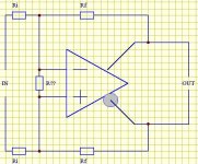
Re: Re: Re: Re: Re: Re: Re: Re: Re: Re: Re: I repeat my Request
OK OK OK. Everybody is asking me questions and I have to go to bed. For now I'll only say that no, I did not make a 500W stage (but a scaled down one) to test the EC and I tested the stage with/out EC without the tracking rails, so I suspect the final version to measure better, as Vce is essentially constant.
Cheers,
Glen
Bob Cordell said:
Hi Glen,
The questions were not pointless.
What value of THD did you get for the output stage at 20 kHz full power? You did not answer this one.
Am I correct in believing that full power is 500W into 8 ohms, driven balanced from both sides?
What kind of a source did you use in order to develope the necessary very large balanced drive signals to measure the output stage in isolation? It would seem like a pretty big undertaking to measure such a large, high-power output stage.
Since the output stage is Class-A, I assume that you would have also had to build the balanced rail-tracking amplifier that feeds its floating rails in order to test it, no?
Cheers,
Bob
OK OK OK. Everybody is asking me questions and I have to go to bed. For now I'll only say that no, I did not make a 500W stage (but a scaled down one) to test the EC and I tested the stage with/out EC without the tracking rails, so I suspect the final version to measure better, as Vce is essentially constant.
Cheers,
Glen
G.Kleinschmidt said:
Incidentally, I have just finished the final schematic for the input/VAS board of my “Death of icky 50W Cordell” amplifier. Here it is, minus the feedback networks and CMV servo/LTP bias:
An externally hosted image should be here but it was not working when we last tested it.
Hi Glen,
Why don't you tell us how you really feel 🙂.
Bob
Time after time "the death of ...." becomes a bit famous, usually with no special result ... 😉

Estuart,
Please maintain a professional attitude when posting. I'm coming in late here, but your previous posts are a bit over the line. Your attitude looks very disrespectful towards other members. I think John and Bob know what they are talking about. True, people may make mistakes, but those and any misunderstandings can be pointed out without resorting to the rather poor attitude you have shown.
-Chris
The RFI paper again
I've read the previously linked RFI paper once more, and I think I have some idea of what it says now.
Here is the linkt to the paper again, in case somebody lost it in the flood of posts:
http://www.ce-mag.com/archive/2000/novdec/fiori.html
Since the paper is concerned with RFI in general, not specifically audio, it seems to ignore the usual mechanism we consider, of RF IM products folded down to the audio band through demodulation due to nonliear transfer function. What it does consider and study empirically is how RFI can shift the Q point of devices and that way even severly modify the transfer function. I am not quite clear about the mechanisms behind this. One claimed reason seems to be that the assymetry in collector/drain current caused by the non-linearity causes this shift (presumably due to non-zero average of the current). However, it seems to me this would not happen unless the RF signal is large enough to almost start clipping, and hopefully we are not dealing with such amplitudes. But there is also a discussion on emitter crowding effects in BJT, which I am afraid I don't understand at all (don't know if I ever did know what emitter crowding is). But similar empirical effetcs are demonstrated also for MOSFETs.
So, it seems to me that this is a problem that is separate from our "usual" RFI mechanism, although related to it. The question then is to what extent this "new" problem is relevant for audio? A steady state RF signal might obviously shift the Q point, but RF signals will probably usually be more complex than that, so I suppose the result would be it induces a signal in the collector/drain current (which might perhaps be described as a wandering Q point). It seems more difficult to predict this phenomenon. I think the question also remains whether this is a problem unless the RF amplitude is very high? And finally, would this effect cause problems in audio? Could it even be the main cause of RFI problems? Or is is it usually negligible or swamped by the "usual" RFI mechanism? I don't expect anybody to have the answer to this, but it seems these questions are interesting, at least for understanding RFI. For curing RFI problems it may not matter, though, since the same methods for minimizing RFI problems seem likely to apply to both kinds of problems.
- Home
- Amplifiers
- Solid State
- Bob Cordell Interview: BJT vs. MOSFET