
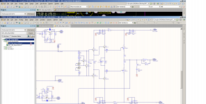
Where is the schematic?
I said that EF and CFP need different arrangements.
To make an assessment one needs to see if it's EF or CFP in a schematic !
I said that EF and CFP need different arrangements.
To make an assessment one needs to see if it's EF or CFP in a schematic !
EFWhere is the schematic?
I said that EF and CFP need different arrangements.
To make an assessment one needs to see if it's EF or CFP in a schematic !
Attachments
triple EF,
The dominant temperature sensitive stage is the output.
You only need to monitor the output Tj
The pre-driver delta Tj is tiny
The driver delta Tj should be low and can often be ignored.
That Vbe multiplier is not two separate compensators. It is one 2transistor compensator.
The dominant temperature sensitive stage is the output.
You only need to monitor the output Tj
The pre-driver delta Tj is tiny
The driver delta Tj should be low and can often be ignored.
That Vbe multiplier is not two separate compensators. It is one 2transistor compensator.
triple EF,
The dominant temperature sensitive stage is the output.
You only need to monitor the output Tj
The pre-driver delta Tj is tiny
The driver delta Tj should be low and can often be ignored.
That Vbe multiplier is not two separate compensators. It is one 2transistor compensator.
so we need to take out the driver Vbe transistor?Or let it be in the same place as the OPS vbe transistor?
Doesn`t the driver vbe multiplier helps in increasing the gate to gate voltage for the mosfet output stages as I have tweaked the values for the driver vbe and found increasing gate to gate voltages for the mosfets?
I have simulated running mosfets at 1.2amp bias per fet using the same circuits but you said it cant be done. So why is the circuit able to do that which you said cant be done.
so we need to take out the driver Vbe transistor?Or let it be in the same place as the OPS vbe transistor?
Doesn`t the driver vbe multiplier helps in increasing the gate to gate voltage for the mosfet output stages as I have tweaked the values for the driver vbe and found increasing gate to gate voltages for the mosfets?
You don't need two Vbe's for a CFP output stage , separate heatsink
for the drivers and vbe.
look at this little 25W amp .. notice the construction -
DIY 25 W Class-AB Power Amplifier
3 devices on the little PCB heatsink are the drivers +Vbe.
The slewmaster only has 2 Vbe's to provide a faster Tc vs. Ic
for that EF3. Both the HK680 and the slewmaster are superior
to a leach (4 diode Vbe circuit).
OS
I'd stay away from the CFP , Randy.
If you want to use your Jfets , the Sansui classic is the way to
go (Kypton V2).
I've repaired 10 of those (OEM) , just main PS caps and compound
on the outputs .... they last >20 years.
VERY durable circuits.
OS
If you want to use your Jfets , the Sansui classic is the way to
go (Kypton V2).
I've repaired 10 of those (OEM) , just main PS caps and compound
on the outputs .... they last >20 years.
VERY durable circuits.
OS
You don't need two Vbe's for a CFP output stage , separate heatsink
for the drivers and vbe.
look at this little 25W amp .. notice the construction -
DIY 25 W Class-AB Power Amplifier
3 devices on the little PCB heatsink are the drivers +Vbe.
The slewmaster only has 2 Vbe's to provide a faster Tc vs. Ic
for that EF3. Both the HK680 and the slewmaster are superior
to a leach (4 diode Vbe circuit).
OS
Bias stability is consuming more than half an hour for me I think using dual vbe multipliers would settle faster. How much time does it takes for you for the bias stability?
Thank you very much for the kind inputs.
Bias stability is consuming more than half an hour for me I think using dual vbe multipliers would settle faster. How much time does it takes for you for the bias stability?
Thank you very much for the kind inputs.
BJT slewmaster (2 vbe) ??
< 1 minute.
"I think" is premature. You actually have to build a REAL output stage
and tweak/observe it to know for sure. Simulations really fall short
in this area.
OS
< 1min is just awesome even 5mins is also excellent.BJT slewmaster (2 vbe) ??
< 1 minute.
"I think" is premature. You actually have to build a REAL output stage
and tweak/observe it to know for sure. Simulations really fall short
in this area.
OS
anyway ill build one and let you know.
Apart from that I have a question regarding driving the mosfets at higher bias consider as class A so I remember Andrew saying that this circuit is not good to drive mosfets. But when I did the sim it was doing 1.2Amp at 30V per mosfet. According to you is there anything to consider to drive mosfets?
Regarding the Vbe multipliers how about using KSC3503 instead of MJE340 as I see the power dissipation is in mW and the main reason is that Im currently using 2sc5171 which is plastic encapsulation as one of the forum member stated that using the plastic encapsulated vbe transistor will take more time to stabilize. But is there any point to consider using low cob transistor as vbe like the one i stated above. Apart from that its small it will fit very well as well as close to the OPS transistor.
I have a question regarding the Large output stage like take 10 pairs of output transistors or even 20 pairs like what nelson uses. what are the challenges to be considered in that aspect like if we take the cob of the transistor take 300pF max so using 20 of them per rail will give about 6nF. Will there by any stability issue?
I'd stay away from the CFP , Randy.
If you want to use your Jfets , the Sansui classic is the way to
go (Kypton V2).
I've repaired 10 of those (OEM) , just main PS caps and compound
on the outputs .... they last >20 years.
VERY durable circuits.
OS
I have just built the circuit Kypton V2 AC coupled and Im getting a strange situation.
Jfet used LSK489.
Got the LED running at 1.65V each and measured across them and Im getting the following output
1. As I increase the voltage from the dimmer stat Im getting all the leds glowing but one of the LED is getting slightly dim after increasing the voltage and just at the time of dimming the idle current through the emitter resistor of the output is shooting exponentially.
Did the following:
1. Increased the source resistor of the jfets to 33ohm from 22ohm. no change
2. changed the jfets to BJT but no change the effect is very similar.
what would be going wrong?
is there any point to consider using low cob transistor as vbe like the one i stated above. .
No point whatsoever..
I have just built the circuit Kypton V2 AC coupled and Im getting a strange situation.
Jfet used LSK489.
Got the LED running at 1.65V each and measured across them and Im getting the following output
1. As I increase the voltage from the dimmer stat Im getting all the leds glowing but one of the LED is getting slightly dim after increasing the voltage and just at the time of dimming the idle current through the emitter resistor of the output is shooting exponentially.
Did the following:
1. Increased the source resistor of the jfets to 33ohm from 22ohm. no change
2. changed the jfets to BJT but no change the effect is very similar.
what would be going wrong?
The problem is really annoying any suggestions?
1. As I increase the voltage from the dimmer stat Im getting all the leds glowing but one of the LED is getting slightly dim after increasing the voltage and just at the time of dimming the idle current through the emitter resistor of the output is shooting exponentially.
Disconnect the output section from the front end, load the Vas with a 10K to ground and diagnose the front end circuit by itself.
yes did got the +ve voltage at supply of 20V i got 19.8V across the 10k load resistor.
Apart from that one of the led is always glowing somehow reduced brightness like about 50% reduced no idea what is happening here. what could be wrong?
Apart from that one of the led is always glowing somehow reduced brightness like about 50% reduced no idea what is happening here. what could be wrong?
- Status
- Not open for further replies.
- Home
- Amplifiers
- Solid State
- Bob Cordell complementary input stage with N channel Jfets