I think having had a read through there’s obviously an issue at output end plus around the TRs and one of the 2SAs. So it’s all leading back to the inductor C3 R10 R13 C4. Plus those 100r resistors. Something is not dropping the voltage. Now LED brand new got 45vdc on it plus no drop either side exactly same voltage. That’s wrong. I’m assuming everything is in VDC? From mains input obviously it is gonna be VAC.
Plus What is EMC 0u1 for? Is it just to stabilise bridge circuit? Plus VU meter circuit via drive to 220k resistor direct link to the +ve on output? On through to inductor. Is that inductor possibly to cause an issue? Not sure what spec it is but I’m sure it’s supposed to be tightly wound which on removing it is not so. Just a thought. But then again it’s just to do with rf.
Anyhow all it can be is there’s a fault with those mosfets. I really cannot see what else it can be. I’ll test every single component once more. But as previously mentioned something is just not stabilising the voltages. The 0v rail again is daft on schematic as it should have a 0v rail around the schematic showing where the components all connect to it and what’s connected to what at what point on that rail. Instead 0v is just floating around all over the circuit with no visible links to the other components. For instance the 0v on transformer is right next to the 0v on output.
Or the new psu caps are faulty possibility.
Basically it could be anything really. So main components to stabilise the voltages is the resistors so again could be a fault there even if showing within there spec does not mean it does not have a fault as it warms up.
Also you have 2200pf PA? Then 820pf STD? Why two different values? Plus R9 lost there 820r PA or 470r STD?
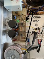
Proper ground ??
Did you made a chassi ground connection or earthed the power lead ?
I checked all the pictures you posted and can't find one with any ground/chassi point but...
You have 3 or 4 ground points on that circuit board so where exactly are you taking the reading from ?
I'm starting to wonder if there is anything wrong with the module or it's just operator error.
They all go to a star ground point on chassis typical valve setup. Less earthing points the better. Yes the mains is earthed pretty critical.
But the other module is also grounded exactly the same so that does not explain why that module is on spec but the other is not. Plus I'm used to taking VAC readings as opposed to VDC readings across a whole circuit. The problem is definitely at the input end and I think the other 100uf cap is bad as again on tapping that the reading shot down to around 6 mV plus again I'm getting a negative reading on it as opposed to positive as per the working module. Plus its at 30mV but the bad side -187.8mV on 100uf cap well out. Plus negative.
Yes readings are taken properly. On output its reference is from 0v rail not grounding point. You don't ground the output on these it goes to 0v. Unless I've got that wrong!
Yeah I think that’s what it is. Re did the transistors all same voltages as other board this time apart from one which is on the leg of the cap.
It's time to start measuring *drop*, when you're measuring *drop*!😉 Instead of measuring each to ground and then subtracting, put one probe on each end of the part to be measured -- one measurement / no arithmetic. If you need something logical to site for a rationale, try 'the meter gives higher resolution'. And stick to DCV exclusively on power amps (except for the inlet fuses, of course).
Now, on to post 201, working back to front.
- the different values for C2 and R9 are to improve RFI rejection and lower gain slightly for PA
- by far the most likely failure mechanism is still cracked foil or 'cold' solder; not sure what you mean by resistors 'stabilize the voltages' -- remember, BJTs are current devices; no symptom you've mentioned so far gives any sign of warm-up issues
- the new main filter caps are fine
- I think you've had it in for those MOSsies since the outset, eh? 😉 maybe set aside testing every part again for now -- every bit of symptom you've described spells 'intermittent connection' of one sort or another
- transformer center tap next to output ground return is smart -- it's the highest-current signal-related connection on the board -- keeps it from corrupting more sensitive sections; pick one ground for all measurements and use it exclusively (except when measuring *drops*! 😉 )
- if the way the grounds are drawn bothers you that much, redraw it; but take a tip from someone whose done that, don't change component designations! 😉
- don't worry about the inductor -- it is outside the feedback loop; anyway, it CANNOT cause an intermittent, full-rail excursion; they generally are NOT tightly wound, its job is to isolate any capacitance the load reflects
- the EMC1's job is to tame the noise caused by the rectifier's turn-off ringing the transformer's leakage inductance
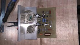
Are TR's4, 5, 6 and 7 mounted almost flush? Likewise the LED? So you can't measure any of them from the component side of the board? A note for the next time that you replace an audio part -- leave it sticking up 4 to 6 mm. Only cost is a very slight decrease in heat dissipating ability.
In the mean time, I suggest that you separate the PCB from that shield plate underneath it. That way you can follow from one logical circuit section to another. The intermittent may even surrender as you probe! 😀
Luckily, separating the angle aluminum heat spreader (what the K135 and J50 are mounted on) from the rest of the heat sink isn't a problem dissipation-wise as long as the 100R's are in place of the fuses.
Cheers
Now, on to post 201, working back to front.
- the different values for C2 and R9 are to improve RFI rejection and lower gain slightly for PA
- by far the most likely failure mechanism is still cracked foil or 'cold' solder; not sure what you mean by resistors 'stabilize the voltages' -- remember, BJTs are current devices; no symptom you've mentioned so far gives any sign of warm-up issues
- the new main filter caps are fine
- I think you've had it in for those MOSsies since the outset, eh? 😉 maybe set aside testing every part again for now -- every bit of symptom you've described spells 'intermittent connection' of one sort or another
- transformer center tap next to output ground return is smart -- it's the highest-current signal-related connection on the board -- keeps it from corrupting more sensitive sections; pick one ground for all measurements and use it exclusively (except when measuring *drops*! 😉 )
- if the way the grounds are drawn bothers you that much, redraw it; but take a tip from someone whose done that, don't change component designations! 😉
- don't worry about the inductor -- it is outside the feedback loop; anyway, it CANNOT cause an intermittent, full-rail excursion; they generally are NOT tightly wound, its job is to isolate any capacitance the load reflects
- the EMC1's job is to tame the noise caused by the rectifier's turn-off ringing the transformer's leakage inductance
Are TR's4, 5, 6 and 7 mounted almost flush? Likewise the LED? So you can't measure any of them from the component side of the board? A note for the next time that you replace an audio part -- leave it sticking up 4 to 6 mm. Only cost is a very slight decrease in heat dissipating ability.
In the mean time, I suggest that you separate the PCB from that shield plate underneath it. That way you can follow from one logical circuit section to another. The intermittent may even surrender as you probe! 😀
Luckily, separating the angle aluminum heat spreader (what the K135 and J50 are mounted on) from the rest of the heat sink isn't a problem dissipation-wise as long as the 100R's are in place of the fuses.
Cheers
Last edited:
Oh, and it might also be worth considering adding inside star lockwashers on at least one of each MOSFET's mounting screws -- top and bottom.
Last edited:
Okay cheers Rick truly appreciated.
Got it all VDC good. Yeah re drawn all 0v around the schematic linking what to what as they say now I know where I am on the tracks.
Grounding pretty happy with that and basically use only one spot for that due to having a plate separating the underside from topside the earth bolt in on the side of chassis so I can just clip on forget about it. Otherwise I’d be flipping it over all time. Yeah could just touch any part of chassis but I like to work from the source.
I did think on removing those plates and copying that picture posted earlier of the same modules without them but then your gonna need the fins on outside of chassis.
Interesting EMC1s job now on start up that module makes a only way of describing is like a ring come boing noise yet other quite as a mouse. But your saying on switch off. Just thought maybe that’s faulty.
Not doing anything today need a rest from it but crack on tomorrow. Yes usually use lock washers but must admit did not on this occasion. It’s definitely losing a connection for sure. I usually in first instant tap things gently see what happens but again left that one out.
I think that also explains why the resistors held up I think it less than 1/4 watt. Not the near on 8 watt initially ha ha. I don’t know. Still certainly been a learning crash course this one.
So that transformer is 45-0-45 I think not sure what amperage it is. Mind you I suppose you could buy a dual supply transformer but then it losses it’s authenticity.
Anyhow I crack on tomorrow.
Resolder these points then clean all of the solder side of the board to remove all the flux.
Inspect all the soldered joints and tracks using some form of magnification.
Preferably of the order of X10

Sid
Inspect all the soldered joints and tracks using some form of magnification.
Preferably of the order of X10
Sid
Blimey you must be reading my mind am using the loupe tomorrow got couple different magnifications up to X30.
Yeah clear mind more logical mind. I suppose easy option would be to get a good quality brand new board made up. Not something I can do plus not sure of cost can’t seeing it being incredibly expensive. Some of the tracks are only about a 1mm width so if you can’t find exact matched part you can’t make a new hole as there would be no track left in place. Just a thought.
Well re soldered some solder joints bit to close using loupe. The zener the hole and track around it missing just been bridged with the leg so new bit copper track in there. Quite a few cold solder joints all re done. Noticed the track with just the big lumps solder on nothing attached to them had also been bridged but you can see the track is not meant to be soldered over as both tracks have a defined stop line between them. So it was connecting to the psu and other psu definitely not meant to be that way otherwise the track would be just one length. So that’s why it was soldered when it did not need to be.
Oh acetone and clean off flux. Quite a bit there as I still use lead solder flows better plus don’t need as much heat less chance damage to components. So will see if done trick or not.
J50/K135
Almost there just need to install the output pair and look for a suitable power supply.
Before someone mentions the transistor yoga, yes it's a budget build and if I'm happy with it I may buy the original transistor critters but for now will have to do.
Almost there just need to install the output pair and look for a suitable power supply.
Before someone mentions the transistor yoga, yes it's a budget build and if I'm happy with it I may buy the original transistor critters but for now will have to do.
Attachments
Wow, RS232! You've certainly been busy 😀 -- Looking good!
Not using the LED CCS, or did I just miss it?
Cheers
Not using the LED CCS, or did I just miss it?
Cheers
Last edited:
Just using the original Maplin part list from their V2 kit (150W)
The board was around 1 hour to do but had to order some components (4/5 days delivery).
The board was around 1 hour to do but had to order some components (4/5 days delivery).
Last edited:
Almost there just need to install the output pair and look for a suitable power supply.
Before someone mentions the transistor yoga, yes it's a budget build and if I'm happy with it I may buy the original transistor critters but for now will have to do.
Did you build the other board as well?
Sid
- Home
- Amplifiers
- Solid State
- BK Electronics mosFET 100 watt modules