Hi Sonnya,
Thanks for those docs! Got them yesterday. Very helpfull, I tried several things, the extra buffer stage, the current source, a diode for biasing etc.
I skipped the current source for it din't help much to linearize the circuit and I din't like the increase in components. Since the current draw will be very little and 20.000uF 5 Volt cap's are cheap, I do not worry about powersupply rejection. So actually the need for current source were gone. Or am I forgetting something?
I am actually pretty satisfied of the performnace it features right now in SIMULATOR. However maybe ther are some pitt falls in real life (heat?)
PS. the BTJ I use now are old ugly, metal can types, but heeee.. I don't know what type to use otherwise..any ideas?
gr,
Thijs
tschrama said:
PS. the BTJ I use now are old ugly, metal can types, but heeee.. I don't know what type to use otherwise..any ideas?
gr,
Thijs
If you have them start with them ... Try build the circuit...
Sonny
Hi,
It has been a while... in the mean time I experimented with the circuit. I did not get it to work. 🙁
It seems that the biasing of the circuit depense too must on the Hfe and/or Vbe of the transistors. I did mach the Hfe's but the circuit still doesn't work.. ouput voltage goes to the supply rail, too much current draw and no signal comming through..
I has designed a new one on my Spice sim which should be less dependent on transistor parameters.
I was hoping on some feedback for this one.
My aim is still a voltage buffer capable of driving 1 Volt RMS into 8 ohm in class A with as little parts and power dissipation as possible.
Greetings,
Thijs
Attachments

I have been following this thread for a while and liked the four transistor version.
I made some minor modifications and will build it this weekend.
It will look exactly like your circuit except all R's=100 will be 220
Input pair will be bc550c/bc560c. Output pair will be BD139/140.
My sim did not like using the BC140/160 combo only. Specially on the input. And output's dissipate 1,5W each, seems a bit much. Using the mods above outputs dissipate less than a watt at 175mA quiescent current. I expect to see some offset at the output, but will take care of that later. If the circuit is OK of course.
Btw, your last version starts to look like a hiraga monstre, doesn't it?
Regards
Hi Rtirion,
Indeed this project is going the look more and more like a Hiraga amp ... I actually am in doubt wheter or not I should use power transistors in the CFP-version and make a real power amplier. But then it would be easier to build a real Hiraga amp.
I like the 4-transistor version the best and I hope you can get it to work!
Goodluck! I hope you let me know how things work out...
gr,
Thijs
Thijs,
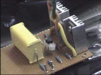
Your 4 transistor buffer design is very viable and yes I have finished building a working prototype. Sound is a pleasant surprise. I will try to post some pictures of the prototype and the test rig for you and all others to see.
Your 4 transistor buffer design is very viable and yes I have finished building a working prototype. Sound is a pleasant surprise. I will try to post some pictures of the prototype and the test rig for you and all others to see.


Hi Rtirion,
Thanks for the nice pictures.
Upon your reply and your e-mail I decided to try the circuit again. This time I AC coupled the input with 1uF and I installed two 22K bias resistors from V+ and V- to the input to bias it half way.. and it works!
Q1/Q4 = bc139/bc140
Iq = about 250mA
V+ = +5Volt
V- = -5volt
source = direct from Philips CD723 CD-player
I found that there is about 300mV offset on the output. Therefore I used a 4700uF cap. to AC couple the output to my speaker.
So far my evaluation has confirmed that the circuit works and that 2Vrms is loud enough for most of my listening situation; allthough I must admid that it is not loud enough for a live-like feel. I cannot yet evaluate the sonic performance since I build a single channel only. The heat dissipation is low. The small black heatsinks I use get only just a little bit warm.
I still not certain about the Iq stabilistion or the Vout stability.
I very interested in your evaluation!
thanks again for your feedback!
gr,
Thijs
I am happy to read that your version is also working.
I had only -22mV offset when I started the circuit. After one hour playing time offset was -16mV. So I do not think I need a capacitor on the output. If I would like to reduce offset further I would put a pot, a resistor and a cap on the input. (like the configuration in Rod Elliot's Death of Zen).
The powersupply I used is unregulated, but kind of large.
Regards
Rtirion,
Your amplifier works very well, but exhibit some thermal instability. I suggest that you mount *all* transistors on the same heat sink, and that you insert small resistors in the emitters of the output devices. You can cancel the offset simply by altering slightly the voltage of one power supply rail.
Regards, P.Lacombe.
I did not find any big thermal stability problems in the circuit. In fact it behaves better than my hiraga le monstre in that area. Still mounting the output devices on the same sink is probably a good idea.
Hi again..
Did you by the way match your transistors for beta or Vbe or not at all?
Dear P.Lacombe,
Can Thermal instability effect also happen on small timescale, like in the sub-20ms audio-range. Something like a bias-shift when loud bass-notes are being reproduces?
gr,
Thijs
Did you by the way match your transistors for beta or Vbe or not at all?
Dear P.Lacombe,
Can Thermal instability effect also happen on small timescale, like in the sub-20ms audio-range. Something like a bias-shift when loud bass-notes are being reproduces?
gr,
Thijs
No, I did not match the transistor pairs for beta of Vbe.
I just got some parts from my junk box, except for the 220 resistors.
As far as I understand the issue of thermal stability, or instability for that matter (which I do not have in the actual circuit), this will show itself as offset drift on the ouput. Since I do not have alarming offset drift figures, and the circuit behaves rather well, I am not too concerned with this.
That does not mean that you can not improve the circuit.
Both input and output transistors are not working in their optimal linear range.
+/- 18mA for a bc550/bc560 is a little bit much. +/- 175mA for a BD139/BD140 is also not perfect.
So the first improvement would be the selection of better (more linear at given Iq) transistors. J.A.Pan makes a few good ones.
You could look at Mr. Haller's recommendations in an other thread on this forum. Take your time to study the datasheets carefully when you select another transistor pair.
Using only one value for all the resistors, except the 47k at the input, is for me part of the fun. This of course imposes some limits.
Hope this helps to develop the circuit even further.
regards
Thijs,
Of course, thermal instability occurs at short time, because of the extreme vicinity of the collector-base junction, which produce heat, and the base-emitter junction, which is very temperature sensitive. All working conditions in which collector-base heat production is variable, are potentially "dangerous".
In fact, only BJT final stages in class AB are concerned, because of the considerable variation of power dissipation, and because idle current stability (and fine adjustment) is essential in order to maintain low crossover distortion.
In class A stages, these effect pass generally for negligible, the resultant distortion (called thermal distortion) is extremely small (but some people claims that they can easily hear that distortion...).
The exact cancellation of the thermal instability in real time is only possible if one can include a temperature sensor in the same vicinity as collector-base junction, which is not a diy job at all :-(
Long term thermal stability is especially important for correct reliability of the appliance, and for security in case of unexpected mains voltage variations and high ambient temperature. (This is why I suggest to improve the thermal stability of the buffer, because I have experienced problems whith similar schematics. Mount *all* transistors, *including drivers*, on the same heat sink).
Regards, P.Lacombe.
Mr. Lacombe,
Thanks for your replys, so far. I have a few questions:
How did you measure the thermal (in)stability in this actual circuit?
Can you explain what equipment you used, and what measurement procedure I would need to at least replicate, validate your findings and conclusions?
Thanks in advance.
Thanks for your replys, so far. I have a few questions:
How did you measure the thermal (in)stability in this actual circuit?
Can you explain what equipment you used, and what measurement procedure I would need to at least replicate, validate your findings and conclusions?
Thanks in advance.
- Status
- Not open for further replies.
- Home
- Amplifiers
- Solid State
- BJT buffer design, can anyone help