Member
Joined 2009
Paid Member
Hi guys,
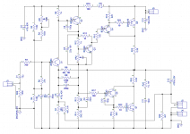
My circuit is a little different to the others here; one of the differences is that I've chosen to take the feedback point before, not after the output cap. My reasoning is that any distortion added to the signal is low-order and therefore benign (might sound better for it!!) and that by closing the feedback loop before the cap, the ULGF canbe pushed higher, because there is less phase-shift in the system, allowing the amplifier to better deal with "nasty" distortion (i.e. cross-over artefacts) at high audio frequencies where available loop gain would otherwise be relatively low in this simple circuit.
Because the cap sits outside the loop, the amplifier is not able to correct LF capacitor induced distortion, which is why I increased the size of the cap to 12,000uF instead of the more usual 4,700uF. The other downside is that damping factor is reduced.
What I didn't account for was the fact that the conventional arrangement helps keep the offset centred at the speaker terminal at startup/turnoff. Turn on thump is pretty terrible with my circuit (since its not under the control of the FB loop) and the problem is exacerbated due to the unusually large output cap, which increases transient time.
My solution was to put a relay in the speaker line with a short turn on delay of about 2 secs. It just happened that I had an eBay speaker protection board conveniently lying around with this feature so I used it. The 100R to ground allows the cap to charge at a sufficient rate that when the relay is closed automatically there is no audible pop.
Its by no means and elegant solution but the unit sounds wonderful and has become a permanent fixture in my one-year-old daughter's bedroom. She goes to sleep listening to it most nights and I often linger to listen also.
I think that if I ever respin these boards I'd move the feedback point to the conventional point and do an A - B comparison, because if there isn't any audible improvement with my approach, the alternative makes more sense.
I installed it on my A/B setup ad compared it to the SymaSym, Honey Badger, Peeceebee and SKA GB150. It held its own against all of them until your get too loud for its power supply. I've listened to it all day and I would not hesitate to recommend it to anyone.
I was asked by a fellow forum member to furnish the layout files for the little Dual channel, single supply cap multilpier. I am attaching the PDF for iron transfer. If anything else is needed please let me know.
Attachments
Member
Joined 2009
Paid Member
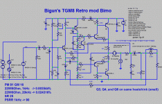
Looking at past schematics I'm guessing that C6 is the dominant pole compensation capacitor at the VAS device. This value can be trimmed to suit your build since it's value depends partly on the parasitics of your pcb layout, the actual transistor devices used and sometimes on the dielectric of the capacitor itself (silva mica reportedly can be a smaller value because of it's higher dielectric absorption ?). You may also find it worth auditioning some values in your set-up because there can be subtle affects on the sound of some amplifiers with changes in the comp. I would look at values for C6 in the range of 47pF to 82pF.
C7 is also part of the feedback compensation. Whereas C6 is usually referred to as lag compensation, C7 is lead compensation. I don't think it needs such a large value as 220pF, I would have thought something in the range of 22pF to 33pF was closer to the mark.
fyi - In a recent amplifier project I compared silva-mica with C0G ceramic as lag compensation and found the ceramic slightly more to my liking (more 'focused') although any differences I heard were very subtle indeed.
Last edited:
Ranchu,Bigun i am attaching the schematic i am reffering to and i also attach my build.
For driver transistors Q4,Q6 i am using HSD669A,HSB649A,(they will be placed in the same heatsink with Q3 BD139 ),for VAS transistor Q2 i am using KSA1381 and for input transistor Q1 i am using 2N5551.
Now my concern is about C6,C7 values,and just a thought of running 2N5551 at 1ma by lowering R6 at about 510~560R
Attachments
Is "lead compensation" the same as input inclusive feedback?Looking at past schematics .................
C7 is also part of the feedback compensation. Whereas C6 is usually referred to as lag compensation, C7 is lead compensation. ...............
It looks to me that C7 is feedback from VAS output back to the input.
C7 is a phase lead as seen in several John Linsley-Hood designs and can help to make the amp more tolerant of difficult (inductive) loads. Agree with Bigun that 220p is *way* too much and I would suggest perhaps 15p or 22p.
The Millar cap, C6, is also too big and will have an audible influence on sound quality. In my version (fully tested) I'm using 22p here with the same output devices and LESS gain.
So if I were to build that circuit and to be on the safe side, I would start with C6 = 33p and C7 = 15p. As a matter of fact, I didn't even bother with the phase lead and it passed clean square waves into inductive dummy loads.
I use only C0G/NPO compensation caps - make sure you use parts that are rated to the full rail to rail voltage swing.
An advantage with this topology is that you can get away with lighter compensation that would be required for the same design with an LTP input.
Last edited:
Now my concern is about C6,C7 values,and just a thought of running 2N5551 at 1ma by lowering R6 at about 510~560R
Reducing the collector load resistor, R6, will increase Q1's Ic (and gm); however, it will also increase the loading on the Q1 collector, pulling the OLG back to about where you started.
If you want to increase the olg of this simple circuit without adding transistors then the better option is to reduce R7 and adjust R8, R9 and C5 to suit. I've built a similar circuit to this with the shunt resistor as low as 10R however the trade-off is that multiple parallel (or series) connected feedback resistors are required to handle the Pd and the shunt cap becomes prohibitively large.
Member
Joined 2009
Paid Member
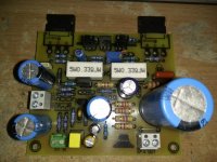
i also attach my build.
Nice looking build !
... You can run the 2N5551 at 1mA but I'm not sure you'll get a huge benefit.
Mod by Bimo
our dear mouna has requested bimo to suggest mods to this retro amp, in another thread. Bimo has posted his mod and I am adding it here.
--gannaji
our dear mouna has requested bimo to suggest mods to this retro amp, in another thread. Bimo has posted his mod and I am adding it here.
--gannaji
Attachments
Last edited:
I'm curious: If 40v or 33v rail, then how many of the TO126 can be replaced with TO92?
Last edited:
Member
Joined 2009
Paid Member
some TO92's can run pretty warm without too many issues, so you may well get away with it - in the original TGM8 the rails were too high, but there are sometimes benefits in using the TO126 because they can be mounted to a heatsink for Vbe and I have also used them as physical spacers between the underside of the pcb and power devices in a kind of stack up.
Thanks!some TO92's can run pretty warm without too many issues, so you may well get away with it - in the original TGM8 the rails were too high...
Mainly, I was wondering if 2N5401 would work for Q2 (vas?)?
Member
Joined 2009
Paid Member
I don't see why not but that device is designed for high voltage rails - how well does it perform at low voltage is something I have no experience with. It's for sure a very nice device.
Very nicely!I don't see why not but that device is designed for high voltage rails - how well does it perform at low voltage is something I have no experience with. It's for sure a very nice device.
I took the shortcut of going by device capacitance as indicator of silicon size and related that to current, to find devices that are neither over nor under utilized. By that means, the ballpark for vas device is 5pf to 9pf, and in order by size, that is: 2N5401, KSP2907A, 2N4403
So, that's a smaller question.
Which of these is optimal on vas?
Member
Joined 2009
Paid Member
the usual approach is to go for smallest Cob, which is a feature of high voltage parts because they need to have thick layers to stand-off the higher voltage - then you add dominant pole compensation using a high quality dielectric for an overall best result. that's the usual approach. it doesn't hurt to look for low noise but that's usually more critical in the first device not the VAS
at low rail voltages you may want to look for signs of quasi-saturation when the signal swings to produce low Vce but I've no experience with looking for such issues, datasheet information on this is sketchy
Daniel, why not try building the thing and then see if you can hear a difference between the devices on your short list ?
- Status
- Not open for further replies.
- Home
- Amplifiers
- Solid State
- Bigun's TGM8 with Single Supply