Hugh, you are the father of this amp. I'm just messing up your design 🙂
The proof is in the pudding, and the pudding is an amp that's built and playing music!
The proof is in the pudding, and the pudding is an amp that's built and playing music!
Hello Minek
greetings PLEASE can you post schematic and component values used in
PCB #57 i would like to try it.
warm regards
Andrew
greetings PLEASE can you post schematic and component values used in
PCB #57 i would like to try it.
warm regards
Andrew
I'm not sure if it matters on class A amps, but on AB amps they say the feedback should be taken from the center point between the emitter/source resistors. Also decoupling caps for op-amp supply should be as close as possible to the supply legs of the IC.
Possibly it could be good to space the outputs further apart, to spread the heat a bit, since it will probably be mounted on a large heat sink?
Just theoretical input, I have never designed a PCB, so please be kind 😉
Possibly it could be good to space the outputs further apart, to spread the heat a bit, since it will probably be mounted on a large heat sink?
Just theoretical input, I have never designed a PCB, so please be kind 😉

Hi Andrew!
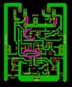
This kind of PCB will be perfect for DIY-ers!
If I may - here is few observations:
1) There is mistake with bootstrap cap (upper one) being connected to Q3.
Emitter of Q3 should be connected to the Source of upper mosfet. The whole arrangement of the upper bootstrap is not correct.
Should be easy to fix.
2) Source resistors are 0.15 Ohm, and they can't be changed to a different value
3) Emitter of Q1 is connected via 100 Ohm resistor to the Gate of upper fet. That should be collector of Q2 instead.
4) You decided to have only one ground connection. This may be a source of hum.
I would suggest either to have 2 grounds: signal ground and dirty ground, and 2 separate wires connecting these grounds to the ground star (or T),
OR - if using only ground wire - use 'lifted ground' with 10 Ohm resistor (to prevent hum).
Input ground of the amp definitely should not be right in middle of the path of big electrolytic filtering caps.
I think 2 ground wires will be more beneficial.
Input circuitry should be connected to 'signal ground', and everything else to dirty ground. See this division in my PCB.
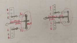
5) Point of output feedback pickup (see my handrawing picture. Right hand side picture shows correct pickup point)
Sam beat me to it 🙂 But I had to draw a picture 🙂
See this link - it's not about audio amps, but the principle is the same.
This kind of PCB will be perfect for DIY-ers!
If I may - here is few observations:
1) There is mistake with bootstrap cap (upper one) being connected to Q3.
Emitter of Q3 should be connected to the Source of upper mosfet. The whole arrangement of the upper bootstrap is not correct.
Should be easy to fix.
2) Source resistors are 0.15 Ohm, and they can't be changed to a different value
3) Emitter of Q1 is connected via 100 Ohm resistor to the Gate of upper fet. That should be collector of Q2 instead.
4) You decided to have only one ground connection. This may be a source of hum.
I would suggest either to have 2 grounds: signal ground and dirty ground, and 2 separate wires connecting these grounds to the ground star (or T),
OR - if using only ground wire - use 'lifted ground' with 10 Ohm resistor (to prevent hum).
Input ground of the amp definitely should not be right in middle of the path of big electrolytic filtering caps.
I think 2 ground wires will be more beneficial.
Input circuitry should be connected to 'signal ground', and everything else to dirty ground. See this division in my PCB.
5) Point of output feedback pickup (see my handrawing picture. Right hand side picture shows correct pickup point)
Sam beat me to it 🙂 But I had to draw a picture 🙂
See this link - it's not about audio amps, but the principle is the same.
Attachments
Last edited:
All good points. Especially spreading output mosfets further apart. They will be REALLY hot, and spreading them is definitely a good thing.I'm not sure if it matters on class A amps, but on AB amps they say the feedback should be taken from the center point between the emitter/source resistors. Also decoupling caps for op-amp supply should be as close as possible to the supply legs of the IC.
Possibly it could be good to space the outputs further apart, to spread the heat a bit, since it will probably be mounted on a large heat sink?
Just theoretical input, I have never designed a PCB, so please be kind 😉
With this rectangular shape of the PCB, mosfets would be better, if they were located at the ends of the 'longer' edge of the PCB.
As for feedback pickup point - it's not about 'middle' of path, but 'away' from that path. High current are flowing via that path,
so there should be another short path from that middle point, and that's where the Speaker Output should be taken from.
Feedback path should be taken exactly from the Speaker Output point. So we are picking Out/feedback from a point where there is no high
current flowing, and voltage is settled.
Last edited:
There is one more thing that would be nice to have on the PCB (what Mjona was asking about):
Q3 - have 2 pinouts for it: one for TO92 transistor, and one for BD140. Some people will want to use BD140 in there.
Q3 - have 2 pinouts for it: one for TO92 transistor, and one for BD140. Some people will want to use BD140 in there.
Looking at the PCB, the 'distortion profile shaping circuit' (RC on the feedback) is connected to the output, but the trace from the VAS is just next to it, so a hole could be added in the VAS trace going to the gate resistor so the builder could try connecting it like in the Alpha too.
I have changed my mind on this point. I believe the need for a slow device in this location is due to differences in frequency characteristics of the output FETs. These have better matching than BJTs but they are not quite perfect. If they were you could use a BC556 instead of a BD140 to bridge a gap.There is one more thing that would be nice to have on the PCB (what Mjona was asking about):
Q3 - have 2 pinouts for it: one for TO92 transistor, and one for BD140. Some people will want to use BD140 in there.
Matching the FETs can be overcome by changing the values of the gate resistors to compensate for frequency differences. In simulations I had to increase these marginally to get a linear gain line in a Tian plot. I made M1 stopper resistor 220R and M2 stopper resistor 150R.
Another complication I saw was that Q2 is not a true buffer stage as the resistors loading the collector and emitter have values that favour the collector. So there is some imbalance with a small degree of gain and alteration of phase inherent in the arrangement.
I can see there has been a lot of effort put into the stability compensation network which has been quite complex however if differences in phase can be sorted out the compensation should be much simpler.
I leave these thoughts with you.
differences in frequency characteristics of the output FETs. These have better matching than BJTs but they are not quite perfect
Since you mention gate stoppers, I think you are thinking about Cis of Fets? Input capacitance?
IRFP (P & N) have similar capacitance. Problem becomes bigger with FQAs or FDAs, N & P differ much more, and gate stoppers may need to
be proportionally adjusted, so R * Cis is the same for both fets.
Another complication I saw was that Q2 is not a true buffer stage as the resistors loading the collector and emitter have values that
favour the collector. So there is some imbalance with a small degree of gain and alteration of phase inherent in the arrangement.
Seems like you have a good grasp of this, can you sim this and propose changes?
Last edited:
If my memory is correct I think you thought it possible to make this circuit stable using only one capacitor to set the dominant pole. To do this the first step is to make the emitter and collector resistors for Q2 need equal in value to avoid any semblance of this transistor operating as a form of a common emitter stage. I propose that various phase correction networks like the one in a box on your schematic be deleted and you make C7 the only capacitor to set the dominant pole - you will need to change the capacitor value. We can then move on to explore other possibilities.Since you mention gate stoppers, I think you are thinking about Cis of Fets? Input capacitance?
IRFP (P & N) have similasted, so R * Cis is the same for both fets.
Seems like you have a good grasp of this, can you sim this and propose changes?
Last edited:
Another complication I saw was that Q2 is not a true buffer stage as the resistors loading the collector and emitter have values that favour the collector. So there is some imbalance with a small degree of gain and alteration of phase inherent in the arrangement.
While this might be true (I did not verify this in the sim), I guess it would also apply to pretty much any simple VAS transistor in any blameless-type amplifier..
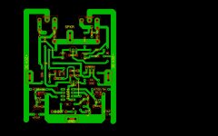
Here is a proposal of bigger, one sided, more DIY friendly PCB.
Wire connections (5 of them) not shown.

Wire connections (5 of them) not shown.
Last edited:
Decided to take mjona's thoughts up and here is my take....
Have added some modified tian probe tools (originally by David Zan which included a differential probe).
They allow for analysing two loops simultaneously.
In the schematic attached the two loops have the following stability:
Main loop: PM 82 GM 22 @ 697 kHz
VAS loop: PM 57 GM 12 @ 5.6 MHz
Seems to simulate ok.
Currently in loop analysis configuration.
To run .trans disable probes (".step param" lines) and enable the ".param Tn=0 Tm=0" line.
Best wishes,
Paul
PS Sorry about image quality. I need a decent software printer to create .png etc directly.
Attachments
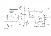
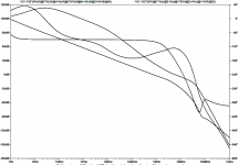
Paul, these are very decent numbers. How is the FFT profile with C12/R22 in place? I guess will try it.
I usually take a screenshot of spice plots (ALT+PrtScr), and then open some image editor (E.g. Paint from Windows) and do CTRL+V (paste).
Sorry about image quality. I need a decent software printer to create .png etc directly.
I usually take a screenshot of spice plots (ALT+PrtScr), and then open some image editor (E.g. Paint from Windows) and do CTRL+V (paste).
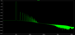
Paul, I repeated your exercise with Middlebrook method, and got the same results.
Just slightly better Thd, and beautiful OLG plot with perfect numbers 🙂
The only drawback I can see is bigger/hotter transistor for the follower (300mW).
I guess that's the reason all commercial amps (that I know) using this topology (op-amp => follower => vas)
used small transistor there, and as a result - slightly imbalanced operations.
I have a feeling Beta Nirvana is going to be a very nice amp!! Especially for winter season.
Attachments
Last edited:
If a TO126 transistor is too big. Increase R8 and R9 in your .asc to 100R.
You are then back to a TO92.
Doesn't make any real difference to the compensation or operation.
You still have balance with regards to Q1.
This amp is interesting for me as it is the opposite of what I normally do.
Probably going to build this. I want to try something new (to me).
Edit: It doesn't seem to like clipping to the negative rail. Maybe something to look at or is it just a simulation issue?
Paul
Last edited:
- Home
- Amplifiers
- Solid State
- Beta Nirvana Class A New Amp