You and I disagree on that one area. I'm using nested fb here to improve harmonic profiling and promote good imaging.
If you ignore the nfb entirely, your THD20k is still 0.0746% however, still high, but again, H2 is dominant and higher orders monotonic.
HD
If you ignore the nfb entirely, your THD20k is still 0.0746% however, still high, but again, H2 is dominant and higher orders monotonic.
HD
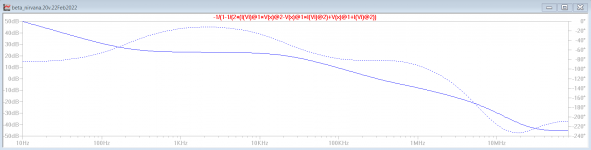
The Tian plot in post 17 was not pretty so what does in look like now.I have slightly changed the IC output circuit, so it takes power from the +15V rail and thereby uses a much larger emitter resistor. Current is unchanged at 3mA, so VAS is unchanged. C9 can be reduced ten times, and this profoundly changes the Bode plot and now GM is 25dB and PM 98 degrees. The 20KHz distortion is not as good (THD is 0.071%) but the profile is unchanged and H2 is easily dominant (-65dB, still much less than a SE tube at -45dB) so this should sound particularly sweet, with very punchy bass below 100Hz.
Minek, I work at a suggested 1 in the AC box for the Tian probe, and yes, my figures are different - one of us is wrong, for sure!
But I'm happy with this, I like your R10/C8 addition and suggest you publish!
View attachment 1028947
Re stability compensation the dominant pole is usually arranged around the VAS which has the greatest voltage gain. Other poles can compete with this and diminish the effect of the dominant pole so if you add capacitors to make progress be prepared to remove them if Tian plot doesn't look right.
You can get around some weird shapes in the plot by making all the electrolytic types equal to 1Farad
Thank you mjona, that does clean out the curves nicely..... this is very stable at it looks.
I will look again at the miller capacitor on the VAS; it could simplify things further.
I'm not sure that beyond about 10MHz the Tian probe is particularly accurate; any comment there?
HD

I will look again at the miller capacitor on the VAS; it could simplify things further.
I'm not sure that beyond about 10MHz the Tian probe is particularly accurate; any comment there?
HD
Last edited:
Bode plot from previous post looks like "closed loop gain", not like "open loop gain" plot.
Here is what expected "open loop gain" plot is supposed to look - in almost perfect amp (OPA192):

Please note - on the left hand side, that gain (in audio bandwidth) ranges from 120dB to 55dB, while phase (in the same bandwidth) stays
flat around 90 degrees. Open loop gain plot is not horizontally flat, but sloping at approx 45 degrees.
Now, here is an example of what actual (measured by Anand on class A amp) "closed loop gain" plot looks like:

As opposed to the "open loop gain", in this case we should see horizontally flat gain plot, at much lower levels (say 20dB) - result of applied feedback.
Now, why bode plot in post #25 looks more like "open loop gain" plot?
I believe this is because so called "local" feedback loop (shaping so called "fft profile") is not that local after all.
This extra loop connects VAS output (which is rail-to-rail swing signal) to one of the inputs of the op-amp.
The impact of this loop is pretty much as significant as the impact of the "global" NFB (same rail-to-rail signal levels).
Tian probe doesn't even see that "local" loop, and that's why the bode plot looks like "closed loop gain".
If you look at bode plot from post #13 - how does it look like?
It looks almost like our "perfect" bode plot (from top of this post).

High levels of gain on the Y axis, phase around 90 degrees, nicely sloped descending line.
And this I what I would expect to see, since we are dealing with an op-amp here.
The same rule should apply to any LTP based amp, just gain levels might be different (slightly lower).
I'm afraid that this "local" feedback taken from VAS output (like in post #25) is skewing the results beyond any usefulness.
It's not Open loop plot, it's not Closed loop plot, it's something in between.
Here is what expected "open loop gain" plot is supposed to look - in almost perfect amp (OPA192):
Please note - on the left hand side, that gain (in audio bandwidth) ranges from 120dB to 55dB, while phase (in the same bandwidth) stays
flat around 90 degrees. Open loop gain plot is not horizontally flat, but sloping at approx 45 degrees.
Now, here is an example of what actual (measured by Anand on class A amp) "closed loop gain" plot looks like:
As opposed to the "open loop gain", in this case we should see horizontally flat gain plot, at much lower levels (say 20dB) - result of applied feedback.
Now, why bode plot in post #25 looks more like "open loop gain" plot?
I believe this is because so called "local" feedback loop (shaping so called "fft profile") is not that local after all.
This extra loop connects VAS output (which is rail-to-rail swing signal) to one of the inputs of the op-amp.
The impact of this loop is pretty much as significant as the impact of the "global" NFB (same rail-to-rail signal levels).
Tian probe doesn't even see that "local" loop, and that's why the bode plot looks like "closed loop gain".
If you look at bode plot from post #13 - how does it look like?
It looks almost like our "perfect" bode plot (from top of this post).
High levels of gain on the Y axis, phase around 90 degrees, nicely sloped descending line.
And this I what I would expect to see, since we are dealing with an op-amp here.
The same rule should apply to any LTP based amp, just gain levels might be different (slightly lower).
I'm afraid that this "local" feedback taken from VAS output (like in post #25) is skewing the results beyond any usefulness.
It's not Open loop plot, it's not Closed loop plot, it's something in between.
Last edited:
Hi Minek,
Nested fb just restricts the open loop at the driver point at the audio band, flattening it out. You don't have to use it of course; most prefer to use only global feedback and that's cool. If you remove it, you get the Bode plot your suggested; straight line from about 90dB where it flattens at 20dB around 550KHz. Then it starts to drop again at about 2.5MHz but I have some doubts that this technique is too accurate at this frequency.
This is your original circuit with the driver emitter 100R to ground, and 220pF to the VAS collector.
GM is 4.2dB, PM is about 30 degrees, not very stable. But THD20k is much better; 0.019% compared to 0.071%.
You can improve the stability by increasing the 220p cap to 470pF; the curves look better, and GM seems to about double.
HD
Hugh, can you attach the .asc file with your simulation?
Numbers, and shape of the plot, as you can easily see in the image in post #26 differ widely from yours.
In my sim (post #13) PM is over 100 degrees, while GM is 9 dB. These are totally workable numbers, actually this OLG plot
is one of the best I've seen so far, which shows the potential of this amp.
I don't believe this is only due to each of us using different kind of probes; the numbers should not differ that much.
I don't have any reasons to doubt my methodology, it worked for me perfectly for many amp builds, and since my sim file and models
are always attached to my posts, anybody can try to reproduce it. This way we can test the same thing and compare results.
I measure OLG, you measure half-CLG, and then of course numbers don't match. Hardly a surprise.
With this kind of measurements, where I have global feedback going through Tian probe, and another feedback loop skipping it,
I can show whatever results I want. I can flatten the curve, I can bump it up, no problem whatsoever.
These issues only apply to the method of measuring/simulating this amp, and getting simulated OLG numbers right.
The topology of the amp is sound, and I believe that regardless of which way the feedback loops are connected (VAS vs OUT),
the results will be the same, or very close. This amp is very tolerant to different variations of R and C values, and from experimenting with
different concepts and values I can tell that it should be stable. It takes whatever you throw at it.
I think the easiest way to tell, would be to build it, and test it in real life.
Numbers, and shape of the plot, as you can easily see in the image in post #26 differ widely from yours.
In my sim (post #13) PM is over 100 degrees, while GM is 9 dB. These are totally workable numbers, actually this OLG plot
is one of the best I've seen so far, which shows the potential of this amp.
I don't believe this is only due to each of us using different kind of probes; the numbers should not differ that much.
I don't have any reasons to doubt my methodology, it worked for me perfectly for many amp builds, and since my sim file and models
are always attached to my posts, anybody can try to reproduce it. This way we can test the same thing and compare results.
It's not a matter what we prefer. It's a matter of "what are we are really trying to measure here".You don't have to use it of course; most prefer to use only global feedback and that's cool.
I measure OLG, you measure half-CLG, and then of course numbers don't match. Hardly a surprise.
With this kind of measurements, where I have global feedback going through Tian probe, and another feedback loop skipping it,
I can show whatever results I want. I can flatten the curve, I can bump it up, no problem whatsoever.
These issues only apply to the method of measuring/simulating this amp, and getting simulated OLG numbers right.
The topology of the amp is sound, and I believe that regardless of which way the feedback loops are connected (VAS vs OUT),
the results will be the same, or very close. This amp is very tolerant to different variations of R and C values, and from experimenting with
different concepts and values I can tell that it should be stable. It takes whatever you throw at it.
I think the easiest way to tell, would be to build it, and test it in real life.
Thanks Hugh!
I have one question - I'm not sure if C10/C11 (bootstrap capacitors) should be connected after or before the tian probe?
In my sims so far, they were NOT part of the feedback loop.
In yours they are connected to Vout. They do provide feedback, but this feedback is not global,
so I tend to think that they should not be part of simulated loop.
This could be one of many differences between mine and your results.
Maybe they should be connected directly to the emitters of the output mosfets (I mean sources).
This way we don't to use 1F values for them.
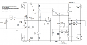
Thanks to Minek for posting the .asc file I have looked at the non-inverting input IC arrangement and due to some minor changes here are some results which may be useful.
At some point I changed the load from 6 Ohms to 8 Ohms and added a 470n test resistor in parallel with the load. The thing that made at lot of difference was increasing the supply rails from +/-20 volts to +/-27 volts. This is so as the collector to base capacitance in a common emitter amplifier depends on the voltage applied at the collector. This capacitance has an inverse relationship in proportion the square root of the applied voltage. That will vary under a.c. signal inputs according to the current passed through the collector load.


At some point I changed the load from 6 Ohms to 8 Ohms and added a 470n test resistor in parallel with the load. The thing that made at lot of difference was increasing the supply rails from +/-20 volts to +/-27 volts. This is so as the collector to base capacitance in a common emitter amplifier depends on the voltage applied at the collector. This capacitance has an inverse relationship in proportion the square root of the applied voltage. That will vary under a.c. signal inputs according to the current passed through the collector load.
Attachments
Last edited:
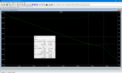
Better results moving the bootstrap points, and Vn is inside the loop now.
Nfb turned off; series resistor deleted.
Max loop gain rises to 93.5dB at 10Hz, and a little more at 27.4dB at 20KHz, compared to the previous 21dB.
This is the new Bode plot, you can see it's much simpler but the figures are not as good; GM 12dB and PM 73 degrees at 2.13MHz:

And this is the 20dBU output at 20KHz into 8R:

Nfb turned off; series resistor deleted.
Max loop gain rises to 93.5dB at 10Hz, and a little more at 27.4dB at 20KHz, compared to the previous 21dB.
This is the new Bode plot, you can see it's much simpler but the figures are not as good; GM 12dB and PM 73 degrees at 2.13MHz:
And this is the 20dBU output at 20KHz into 8R:
Attachments
Very solid results so far.
I have few general observations about this (and other) amps - what I noticed when doing simulations.
1) Minimum "decent" Phase Margin value is 45 degrees. I would not build an amp that can't do 45 degrees or more.
Perfect value that we would like to achieve is 60 degrees. An amplifier with PM < 60 will ring for longer and an amplifier
PM > 60 will take a longer time to rise to the voltage step's final level.
The higher power we want to achieve (and have decent Slew Rate), the more importanter (sic!) it is to get closer to 60 degrees.
For low (output) power (and lower Slew Rate), 45 degrees will be just fine.
2) Optimal Gain Margin seem to be 5 - 15 dB. I target number around 10 dB.
"A system with a large gain margin and phase margin is stable but has a sluggish response, while the one with a
small gain margin and phase margin has a less sluggish response but is oscillatory."
So I guess we don't want gain margin to be too high either.
Different people target slightly different numbers. For example in this thread.
All in all, I would stick to the range of 10 -20 dB, and we should be good.
3) Beta Niravana amp turned out to be difficult one to get nice handling of square waves.
So all the RC values in my sims are a compromise between Thd level, FFT Profile, PM/GM, square waves shape, and OS power consumption
4) Simulate with output RL network or without it?
I tend to skip RL in the output for the simulations. Why? Because it can possibly hide problems with the amp - and that's fine, that's
what it's supposed to do in the actual amp - correct things.
But when simulating OLG or square waves, I don't want to hide anything, I want to see all the problems, and fix them 'organically'
within the amp. Once it's all good and nice, RL network can be added.
Some lousy amps will not simulate well without RL network, but this amp is not one of them 🙂
I would appreciate any thoughts or corrections to my observations here...
The thing that made at lot of difference was increasing the supply rails from +/-20 volts to +/-27 volts.
This amp is sensitive in terms of idle current applied to OS. By increasing rails voltage you might have affected
the idle current. My guess is that source resistors may need to be adjusted if rails voltage is changed...
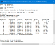
I was verifying two different methods of simulating open loop gain: simpler method used by me,
and Tian method used by Hugh.
Attached two .asc files for both methods. Schematic of the amp is identical in both cases.
Also attached OLG results. They are identical. Almost exactly the same numbers.
So it looks like both methods are working just fine, and results are reproducible (with all other things being equal).
In both cases:
Phase Margin: 113 degrees
Gain Margin: 13 dB
Thd at 1kHz (full power): 0.00035 %
Thd at 20kHz (full power): 0.0869 %
Square waves: very good
Idle current: 2.36A
Dissipation per Mosfet: 46W
FFT profile - ignored for now, since we can shape it whichever way we want using Hugh's RC feedback method
I'm simulating amp with 20V rails (that's my PSU, and that's what I'm planning to build).
Hugh is simulating amp with 27V rails.
Attachments

Last edited:
I agree with that. Re the simulation Tian plot looks strange and I think the bootstrap capacitors pass feedback in positive phase these should somehow be connected somehow to the probe and the feedback connection rather than the output.This amp is sensitive in terms of idle current applied to OS. By increasing rails voltage you might have affected
the idle current. My guess is that source resistors may need to be adjusted if rails voltage is changed...
Some years ago I had a problem simulating an amplifier with a bootstrap collector load on the VAS and another contributor, Bimo, I think found a work around method to deal with this. You might like to look him up and see if he can help.
It took a little longer than normal for my simulations to run - for me usually a sign of a need for more work.
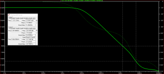
Attached is a Tian plot for a circuit giving close to the ideal phase margin you mention - there are no humps or notches in gain line.
Attachments
For me simulations are instantaneous. You are right, I noticed the same thing - the longer sims take, the more likely there is something wrong...It took a little longer than normal for my simulations to run - for me usually a sign of a need for more work.
But in this one, everything was quick...
I think the bootstrap capacitors pass feedback in positive phase these should somehow be connected somehow to the probe and
the feedback connection rather than the output
To be honest - I don't know. I rarely use bootstraps like this..
But, these caps do not qualify to be a treated as "global feedback" in my eyes.
And we are using two of them, for upper and lower Fets.
In most of similar amps, there is only one bootstrap used (E.g. Aleph amp).
Using 2 bootstraps is not as common. Perhaps Hugh can tell us the story behind this..
I recall that in the original AN thread there was discussion about this (2 bootstraps vs 1), but I can't find it now...
Attached is a Tian plot for a circuit giving close to the ideal phase margin you mention - there are no humps or notches in gain line.
Yeah, this plot looks perfect. One thing I noticed - much lower levels of gain (Y axis). This tells me that this plot was done for an amp
with traditional LTP input. No high gain op-amp.
Within audio bandwidth this plot ranges from 42dB to 28dB only (14dB difference).
Typical op-amp will start from over 100 dB.
With op-amp here, we are getting much higher levels of gains in the open loop, which makes humps and bumps more likely.
It's not easy to handle this levels of gain for all frequencies.
But our plot doesn't have to be perfect. It needs to be good enough.
It should roughly correspond to the bode plot of the op-amp used in the amp.
Last edited:
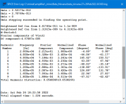
Here is 27V version.
The only components that were changed:
a) source resistors (0.22 Ohm now)
b) bootstrap resistors swapped (1k5 <-> 1k)
c) bootstrap caps (100uF -> 220uF)
d) gain increased (R4=1k2)
e) Zener resistors (R5=R14=1k2)
Phase Margin: 107 degrees
Gain Margin: 14 dB
Thd at 1kHz (full power): 0.00892 %
Thd at 20kHz (full power): 0.0540 %
Square waves: very good
Idle current: 1.7A
Dissipation per Mosfet: 45W
FFT profile - ignored for now, since we can shape it whichever way we want using Hugh's RC feedback method
Attachments
Thanks Minek,
Good results!
Two bootstraps ensure that driving the mosfets gates will dominate because the loading will be very high.
They also tend to load up at very high frequencies which can make the amp easier to stabilise.
In my later .asc I took the bootstrap inside the Tian probe, so I assume it included them in the feedback loop.
I had the impression that R3/C14 is not needed.
I was very surprised that the Middlebrook method was almost identical to the Tian.
Perhaps this is the time to lay out the pcb.......
HD
Thanks Hugh! I think it works very well with 2 bootstraps.
Not sure what is giving hard time with square waves tests, I suspect the CCS/current limiter.
But now square waves are behaving fine.
About 2 years ago, when I tried Tian method, it didn't work out for me, so I settled for the Middlebrook,
and never tried Tian again... I guess I was doing something wrong. Thanks for us your working example!
I'm sure some DIY members will recognize where it came from..
This configuration was used in a few HiFi amps in the late 70s (op-amp, 100R to the ground, follower, RC, VAS transistor),
and R3/C14 was always used. But let's try to see what happens without them.
As for the PCB - I already have one design almost ready. But this design may not be very DIY friendly.
I have specific requirements for my build/chassis...
What do you think about designing backward compatible (with old AN) PCB?
I'm not a big fan of these molex connectors (and connecting mosfets on long wires), so I wouldn't use it for myself,
but it would be convenient for other builders.
Not sure what is giving hard time with square waves tests, I suspect the CCS/current limiter.
But now square waves are behaving fine.
I was very surprised that the Middlebrook method was almost identical to the Tian.
About 2 years ago, when I tried Tian method, it didn't work out for me, so I settled for the Middlebrook,
and never tried Tian again... I guess I was doing something wrong. Thanks for us your working example!
Will look into them. To be honest this circuit (follower + VAS) is already simplified from the original amp I borrowed it from 🙂I had the impression that R3/C14 is not needed.
I'm sure some DIY members will recognize where it came from..
This configuration was used in a few HiFi amps in the late 70s (op-amp, 100R to the ground, follower, RC, VAS transistor),
and R3/C14 was always used. But let's try to see what happens without them.
As for the PCB - I already have one design almost ready. But this design may not be very DIY friendly.
I have specific requirements for my build/chassis...
What do you think about designing backward compatible (with old AN) PCB?
I'm not a big fan of these molex connectors (and connecting mosfets on long wires), so I wouldn't use it for myself,
but it would be convenient for other builders.
Last edited:
- Home
- Amplifiers
- Solid State
- Beta Nirvana Class A New Amp