I found no difference in the metrics with R3/C14 so best to drop them.
Different purpose in the output of the IC compared to collector of VAS driver.
I did not design the DIY pcb; it was done by JPS. Like you I don't much like molex connectors for DIY - they are used in industrial design - and enable cards to be removed easily in the field for replacement to keep the circuit running. Not needed here although they are useful to clip up the mosfets which are located elsewhere on a heatsink.
I would ask Prasi for this, he does beautiful boards and easy to build. I would not choose to back compatible this with the AN. It's its a very new amplifier.
I am a fan of the nested fb circuit; it can be permitted, used or not used as preferred.
Good project, thank you for your hard work,
Hugh
Yeah, I also don't see a difference...I found no difference in the metrics with R3/C14 so best to drop them.
Few questions:
a) any particular reason to use R 180k from the input to ground? Value this high was messing up square waves, that's why I lowered it, otherwise I didn't notice any difference vs 22k
b) CCS 220p is better than older version R + C ? Which one should we retain?
Hi Minek,
a. R1 resistor references the input to ground, nothing more and could be left say 150k. The input impedance to the jfet input of the IC would be multiples of megohms, and R2 with C2 sets the corner for the low pass and this is what interferes with the square wave. I'd use R2 as 1K and C2 as 470pF but R3 could be around 22k as it ensures no EMI ingress and gets the source a decent load. 22k it is then.
b. I think we should hold C11 across base and collector of the sensing BD140 at 220pF. Together with the slower BD140 this stops the active CCS from hiking up and down with oscillation. The voltage at the load will still be set by the nmos, but it's smart to stop the active CCS from oscillating.
I tried a folded cascode driving the VAS as we've discussed in emails. No dice. Can't get it to work well, and in event the current demand from the IC is hundreds of uA higher and takes the output stage out of Class A. With about -900mV on the IC and a very low output voltage and current output we skew the output stage, and as long as the current demand is less than ten times less than the quiescent (which I'm guessing is about 2mA or thereabouts) it should operating in single ended mode. Leave it is I say, it's the best we can do.
Cheers,
Hugh
Last edited:
OK. I can try to make cascode to work, so far I was focused on this version..
There is many ways to arrange this cascode..
CCS transistor in theory should be slower (as Hayk K pointed out), however in the sim, faster ones gave better results.
Selection of this transistor actually slightly affects OLG and Thd...
KSA992, 2N5401, BD140 have been used in different builds.
Since I used 2N5401 in three AN builds and it worked fine, that's why I used 2N5401 in this schematic.
then everything stabilizes nicely. Perhaps it's related?? Will spend little more time on this.
There is many ways to arrange this cascode..
CCS transistor in theory should be slower (as Hayk K pointed out), however in the sim, faster ones gave better results.
Selection of this transistor actually slightly affects OLG and Thd...
KSA992, 2N5401, BD140 have been used in different builds.
Since I used 2N5401 in three AN builds and it worked fine, that's why I used 2N5401 in this schematic.
I noticed that when testing square waves, in the 1st 100ms there is ringing in the upper part of the wave, then in the lower, andslower BD140 this stops the active CCS from hiking up and down with oscillation.
then everything stabilizes nicely. Perhaps it's related?? Will spend little more time on this.
Last edited:
For me simulations are instantaneous. You are right, I noticed the same thing - the longer sims take, the more likely there is something wrong...
But in this one, everything was quick...
To be honest - I don't know. I rarely use bootstraps like this..
But, these caps do not qualify to be a treated as "global feedback" in my eyes.
The problem with Tian simulations applies only to bootstraps used for increasing collector loads in common emitter amplifier stages. The circuit responsible for the images I posted includes one for a purpose other than for "global feedback" - a point I had overlooked in earlier comments. The first stage in this circuit is a single transistor with a constant current collector load, so as you correctly conclude not an op-amp.Yeah, this plot looks perfect. One thing I noticed - much lower levels of gain (Y axis). This tells me that this plot was done for an amp
with traditional LTP input. No high gain op-amp.
Within audio bandwidth this plot ranges from 42dB to 28dB only (14dB difference).
Typical op-amp will start from over 100 dB.

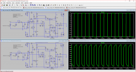
I looked at the 27V version several times to look at the square wave response and to compare the results with the modified version I attached to post 31. I don't like to see phase response not trending downward with gain as shown in the example previously discussed. In the attached image the version as above gives a decent square wave with a 680nF test capacitor in parallel with the output load.Here are 2 versions (20V and 27V) final (for now) of the amp sim files.
That in your latest simulation, even without any test capacitor loading the output is distorted, and remains so if the square wave test is done at 20kHz.
It is unusual to see square waves so straight as in the attachment in post 31, I think that is attributable to the op.amp and some elements nested feedback loops are incompatible with poles in the discrete component section. So should we take a more direct approach or adhere to an approach needing a problem that appears not to be there.
Attachments
You need to disconnect optional RC circuit (C9/R5) for "profile" shaping.
It seems that these rounded square waves are side-effect of it.
This could be the reason why you've never seen simulated square waves plot in the original AN thread 🙂
In you upper schematic this RC is disconnected, and the lower one has it connected.
In real life it is not that bad, I think simulation is making it look worse than it is.
My AN was showing fine squares on the oscilloscope:
Last edited:
I will try it today!
But I know the result... the and stability are changed but not much by much.
I would never use nfb unless there were a good reason and I did discuss it some time ago.
When you have the IC AN running, try it with and without. You should hear it then!
Very nice pcb Minek. I will contact Prasi see if he is interested doing a DIY pcb for us....
HD
I got the wrong end of the stick here, I left these components unconnected in my simulation and put them back when I saw them in a box on your later simulations. Anyway I had not finished with a Tian plot as indications were there was a peak at high frequency. I had your C7 at 100pF and changed that to 15pF you have arrived at and bingo.Y
You need to disconnect optional RC circuit (C9/R5) for "profile" shaping.
It seems that these rounded square waves are side-effect of it.
This could be the reason why you've never seen simulated square waves plot in the original AN thread 🙂
In you upper schematic this RC is disconnected, and the lower one has it connected.
In real life it is not that bad, I think simulation is making it look worse than it is.
My AN was showing fine squares on the oscilloscope:
View attachment 1029810
You have to be happy with the square waves on your scope and to add to your joy the simulation supports this.
Attachments
You need to disconnect optional RC circuit (C9/R5) for "profile" shaping.
It seems that these rounded square waves are side-effect of it.
This could be the reason why you've never seen simulated square waves plot in the original AN thread 🙂
In you upper schematic this RC is disconnected, and the lower one has it connected.
In real life it is not that bad, I think simulation is making it look worse than it is.
My AN was showing fine squares on the oscilloscope:
View attachment 1029810
I disconnected these parts which appeared in a box in your simulations. Later on, and I assumed they were supposed to be there. Anyway you have to be happy with the square wave tests which look in line with the simulations. I The one I did not show in post 31 had a notch in it that needed straightening out changing your C7 from 100pF to 15pF sorted that out. Now that you have done that the stability margins are fine - Gain 14dB Phase 79 degrees see attached.You need to disconnect optional RC circuit (C9/R5) for "profile" shaping.
It seems that these rounded square waves are side-effect of it.
This could be the reason why you've never seen simulated square waves plot in the original AN thread 🙂
In you upper schematic this RC is disconnected, and the lower one has it connected.
In real life it is not that bad, I think simulation is making it look worse than it is.
My AN was showing fine squares on the oscilloscope:
View attachment 1029810
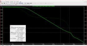
In these OLG plots I see that:
a) you flattened the 1st part of it (0 .. 200 Hz). Before it was sloping from 120dB to 65db, now it's flat from 75dB to 65dB.
After 200Hz it's pretty much the same plot as before.
b) phase margin was flat before at approx 90 degrees from 0Hz to 100kHz (which is good),
in the new plot, PM starts at 0, and reaches 90 degrees only after 1kHz, so we see here little bit more variation..
I suspect you applied too much feedback, hence the flattening of the gain plot below 200Hz
So basically the gain plot is flatter, because gain of the input stage has been tamed (perhaps too much ?).
Attachments
In these OLG plots I see that:
a) you flattened the 1st part of it (0 .. 200 Hz). Before it was sloping from 120dB to 65db, now it's flat from 75dB to 65dB.
After 200Hz it's pretty much the same plot as before.
b) phase margin was flat before at approx 90 degrees from 0Hz to 100kHz (which is good),
in the new plot, PM starts at 0, and reaches 90 degrees only after 1kHz, so we see here little bit more variation..
I suspect you applied too much feedback, hence the flattening of the gain plot below 200Hz
So basically the gain plot is flatter, because gain of the input stage has been tamed (perhaps too much ?).
Assessment of OLG is covered in SPICE tutorials on Bob Cordell's website where he has a zip file covering a battery of tests in the main field. One method is shown in the image attached.
To continue I was not able to reduce the phase margins very much by the means I use with Bode plots such as increasing closed loop gain by reducing R4 which decouples the feedback to earth to 470R, and reducing the current passing through the VAS transistor and hence the trans-conductance of this stage.
Otherwise C7 can be reduced in value however this is pretty skinny and the path from between the collector load on the VAS transistor and the IC inverting input could be layout critical. I made that 12pF which resulted in a gain margin of 12 dB and a phase margin of 68 degrees.
If you can live with this then you will have enough closed loop gain such that input controls could be passive - for volume and switching.
C7 (along with C9/R5) is also a part of profile shaping circuit, and as such is not really needed, if someone is interested in 'pure' and 'organic'
fft profile. Without C7, H3 will be slightly higher than H2, which Hugh wanted to avoid.
It is possible to compensate this amp without C7 at all, but the harmonics profile won't be what it is.
fft profile. Without C7, H3 will be slightly higher than H2, which Hugh wanted to avoid.
It is possible to compensate this amp without C7 at all, but the harmonics profile won't be what it is.
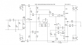
I consider this PCB as ready (at least for me), and I'm going submit it for production in a week or so (have
2 more other PCBs to finish and want to submit them in one batch).
D3,D4,R10 to be soldered under the board.
If anybody wants gerbers or sprint layout file, pls let me know. For DIY only.

2 more other PCBs to finish and want to submit them in one batch).
D3,D4,R10 to be soldered under the board.
If anybody wants gerbers or sprint layout file, pls let me know. For DIY only.
Last edited:
Nice work on the pcb.C7 (along with C9/R5) is also a part of profile shaping circuit, and as such is not really needed, if someone is interested in 'pure' and 'organic'
fft profile. Without C7, H3 will be slightly higher than H2, which Hugh wanted to avoid.
It is possible to compensate this amp without C7 at all, but the harmonics profile won't be what it is.
The but ... statement would be a bummer for prospective builders who see the profile of the harmonics as the key attraction of the design. You mentioned how stability margins affect sound in an earlier post where the phase margin is in the vicinity of 65 degrees where the transient response would tend to being more agile. This can be achieved by reducing both values of the feedback divider network resistors, while increasing the closed loop gain, plus a small change in the value of C6.
Also in post 43 Hugh mentions what I see as a red flag over the choice of transistor used for Q3 - he used a BD140 rather than 2N5401 as he wanted a slow transistor to avoid oscillation. I have tried an MJE350 in a simulation - slower than a BD139 could be another option.
Anyway I see you have an ebc pin layout for Q3 on your pcb to take a 2N5401. 2N series transistors used to be available from over the counter outlets like Jaycar and Altronics or online from warehouses like RS Components. These seem to be disappearing from stock lists and 2N5401s are no longer sold by these places.
For future proofing and with new builds substitutes from the BC556, 557, and 560 range available from over the counter stockists could be tried. These have a cbe pin layout and they will still need your added in components to slow them down.
These are not needed with BD140 and MJE350 which are available from such stockists - at least here in New Zealand and in Australia. Should you change the pcb to match whatever pin layout for cbe or bce?
Hugh has a large following and those who want to keep faith with his thinking. If the layout was able to accommodate both pin layout options that could have some influence over decisions in going ahead to build the amplifier.
I will save giving the details re optimizing the phase margin for another time.
Last edited:
Also in post 43 Hugh mentions what I see as a red flag over the choice of transistor used for Q3 - he used a BD140 rather than 2N5401 as he wanted a slow transistor to avoid oscillation. I have tried an MJE350 in a simulation - slower than a BD139 could be another option.
a) First off all, I don't really know what Ft of BD140 is. I checked many datasheets for BD140, all that I could find, but Ft is never published.
As far as I can tell - old BD140 used to be slow, but for modern BD140 Ft could be anything...
Slowest transistor I could find in my stash with confirmed Ft=50Mghz min is MPSA92. So perhaps this is good candidate.
b) Contrary to claims that slower transistor is better for the CCS, the sim (Thd and OLG) worked slightly better with transistors other than BD140.
c) My AN builds worked perfectly fine with 2N5401.
So taking all of this into account, my plan is to try MPSA92 in my build, and then 2N5401.
My guess is that both of them will work just fine.
KAS992 is also confirmed to work fine. So most likely pretty much any pnp BJT will be ok.
These seem to be disappearing from stock lists and 2N5401s are no longer sold by these places
I just received batch of 2N5401/2N5551 from Mouser 3 weeks ago. Not sure if they are stocked now, but they are not obsolete.
I have 100s of them, and I'll be using them 🙂
Let me know if you need some.
Any builder is free to use whatever transistor he wants. I'm only giving suggestions.
Actually they are not even suggestions, just opinions 🙂
I guess at some point we need to have BOM, and we could give different options in there...
Hugh has a large following and those who want to keep faith with his thinking.
If the layout was able to accommodate both pin layout options that could have more influence over decisions in going ahead to build the amplifier.
You are right; so perhaps in the bigger, DIY friendly PCB layout we can accommodate different pinouts.
My PCB is really small, and I don't want to squeeze big BD140 in there, if MPSA92 will work just fine.
If Prasi can design bigger PCB, more DIY friendly, that would be great. If he can't - I can do it. Or anybody else.
Michael, if you want, I can give you sprint layout PCB file, and you can play with it. Perhaps fuses can be removed, and that would
release a lot of space for BD140.
The but ... statement would be a bummer for prospective builders who see the profile of the harmonics as the key attraction of the design
You are right.
That's why C7 is retained as is. It's not optional, and the current sim and PM/GM numbers are good with it.
If you remove C7, and leave everything else 'as is' - will do no good; C7 is an integral part of the sim, and can't just go away without making
major changes to the overall amp compensation.
We are not removing it. H2 will be higher than H3 - that's the signature characteristic of AKSA amps we definitely want to keep.
C9/R5 does not affect PM/GM numbers almost at all (when connected from OUT instead of VAS, and with reasonabale values),
so anybody who wants harmonics to be elevated and audible (above 90dB), can use them.
The values Hugh was using were 330k and 4n7 (or 3n3).
Last edited:
Good answer, very reasonable.
It is your design Minek, I'm standing to your side with the solder roll and much of this amp has been reconciling our Tian probe so reality and simulation meet. That's been very helpful for me.
I also suspect that with the 220pF from base to collector of the sensing transistor any pnp would be fine, and I can confirm that the speed of the BD140 is VERY hard to find in the datasheets and could be anything...... I'd assumed with a heavy 1.5A collector curent the die was much larger than most and this could reflects a lower ft.
Much of the FFT of this amplifier is created in the output stage, that is where the magic is. It is a pseudo-single ended FFT. It would be good engineering to use a good IC front end if only for the offset control, very low distortion and low parts count.
HD
- Home
- Amplifiers
- Solid State
- Beta Nirvana Class A New Amp