lumanauw said:Hi, MikeB,
I saw some make diamond buffer by attaching collector of Q8 to emitor of Q1 (C-Q7 to E-Q4), instead to rails. What properties are improved this way?
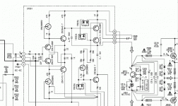
That has similar effect like my q2/3. The effect is, that Vce of the inputdevices (q7/8) becomes nearly constant.
This way these devices creates nearly zero distortion, as Vce and Ice are close to constant. By definition these devices can no longer distort.
Also, supplyvoltage can be reduced. Diamond buffers without this change need much higher supply voltage to reduce percentual voltage fluctuation (Vce) on the input devices.
Mike
Hi, MikeB,
Thanks 😀 It's clear now. I tought it was somekind of feedback/EC, but failed to see where this mechanism works. It's for constant voltage.
If something is modified like this (R13-R11), is the purpose still for constant voltage or something else?
Thanks 😀 It's clear now. I tought it was somekind of feedback/EC, but failed to see where this mechanism works. It's for constant voltage.
If something is modified like this (R13-R11), is the purpose still for constant voltage or something else?
Attachments
Hi Mike,
Is it a good idea to connect Q7/8 collectors to output...it will work in sim, but with real devices (BC550/560) with Vcb near zero?
Is it a good idea to connect Q7/8 collectors to output...it will work in sim, but with real devices (BC550/560) with Vcb near zero?
Re: Surprise
I'm definitely surprised to see this too. I knew there are a few Malaysians and Indonesians browsing this site but I'd never expect one from Penang specifically. 🙂
MikeB, I tried simulating the Calibu circuit you posted with floating cascodes (Q2 and Q3 addition) and they seem to be oscillating with 1kHz Squarewaves. Some excessive overshooting was observed.
ttan98 said:TzeYang,
I am plesantly surprised to see a Penangnite visiting this forum. I am an ex-Penangnite, but still a Malaysian.
cheers.
I'm definitely surprised to see this too. I knew there are a few Malaysians and Indonesians browsing this site but I'd never expect one from Penang specifically. 🙂
MikeB said:
q2/3 between the collectors of q7/8 and the rails are the difference to a normal diamondbuffer and are floating cascodes. These heavily improve performance of the buffer.
Steven is a member of this forum.
Mike
MikeB, I tried simulating the Calibu circuit you posted with floating cascodes (Q2 and Q3 addition) and they seem to be oscillating with 1kHz Squarewaves. Some excessive overshooting was observed.
Mike,
I agree about the improved specs but I question the sound. A similar idea is to tie tie the collectors to the output emitter resistors(often used in Mark Levinson equipment) but I have found it to hurt the sound despite improved measurements...........it probably warrants further investigation.
Regards,
Jam
Interesting discussions, thanks.
you know, this is remarkably like an article on cascode design (http://www.passlabs.com/pdf/articles/cascode.pdf)
I've been pouring over this thing, and have come to some understanding. Although there is merrit in this design, a couple of things come to mind right away: this circuit is extremely dependant upon jfet choice. That upper jfet sets the bias current, which will vary by jfet choice (due to self bias nature), and probably temperature.
Did someone say the sound quality isn't so hot? Interesting.
So back to the drawing board?
lumanauw,
...............I am willing to bet that stability was part of the problem.........to many cascodes and compensation can become a nightmare.
Jam
...............I am willing to bet that stability was part of the problem.........to many cascodes and compensation can become a nightmare.
Jam
getting back to the original thread topic, sort of, can a discrete opamp beat the sonic quality of a monolithic device?
So far, my discrete opamp has 11 transistors, 2 diodes and a hand full of R and C. In surface mount, I don't think this will be very large footprint. The offset voltage is around 300uV and is temperature stable from at least 0 to 70C. Slew rate simulates to around 25V/us. Noise floor when driving 1kHz, 1V, into 1K load is around -180dBv. THD is 0.0005% with souce impedance of 20k.
Definitely not minimalist design though.
Very interesting thread here. I'm wondering if it would be better to use regular cascodes instead of the floating ones. What advantage do those render?
Designer like John Curl, Nelson Pass seems to prefer static voltage divider referenced cascodes in their designs. Some Japanese amps use floating cascodes. Maybe they differ mainly in sonic performance?
As Mike explained, the floating cascode fixes the voltage across the active device. If that device also passes constant current, then clearly its Vbe cannot change since it's in constant power.
A device operating in constant voltage AND current delivers rock solid Vbe, therefore input/output transfer is merely an arithmetic step function. In the EF configuration, this is the ideal, and it defines zero distortion.
The Cadibu is clever indeed, but the current amplifier on the output is still subject to the same old EF transfer function, small, but measureable.
Thanks Mike, good circuit,
Cheers,
Hugh
Yes indeed. To me it looks kinda' like a feed-forward voltage compensation, but i might be wrong. Clever circuit, i might try one myself.
I have a question about the Jfet version. Why does it break into oscillation if the 47 pF cap is removed?
emanuel_hr said:I have a question about the Jfet version. Why does it break into oscillation if the 47 pF cap is removed?
Take a close look at that circuit. You may notice a loop formed by:
fet Drain to
pnp emitter to
pnp collector to
npn base to
npn collector to
fet Source
Under the right circumstances, it'll oscillate. That cap forces a pole on that network, which seems to keep it from oscillating.
hmmm, the more I think about it, the more I think that last description is wrong.
Maybe the drain-emitter-base-source loop is the culprit, instead. The current at the drain is in-phase with the base current. Then it gets gained up by the jfet and eventually oscillates after a couple times around the loop. At high enough frequency, that 47pf cap shunts to the minus supply through the npn.
Maybe the drain-emitter-base-source loop is the culprit, instead. The current at the drain is in-phase with the base current. Then it gets gained up by the jfet and eventually oscillates after a couple times around the loop. At high enough frequency, that 47pf cap shunts to the minus supply through the npn.
The current doesn't get amplified by the jfet. The pnp transistor plays a double role here: It keeps the Vds constant to about one Vbe drop and it never turns on too hard. Secondly it biases and controls the current sink/source formed by the npn transistor in order to obtain a kind of push-pull output current. However I still don't understand how does it oscillate at any frequency without that cap.
I won't pretend to completely understand the mechanism, but you know what? I think the parasitic capacitors in the jfet are coming into play. In my simulation, it's not the 47pf cap that stops the oscillation - it's the 10pf dude on the gate.
It appears that the pnp gets shut off, as the Vds drops to around 0.25. Then looking at the gate, the voltage swings wildly, in a saw-tooth wave from +8 to -8. The only feedback path is via those parasitic caps, from gate to drain and from gate to source - yes?
BTW, this thing only oscillates when the caps are out, and the source is zero - at least on my simulation.
I'm, too, quite split minds on this circuit. It seems to work, but it is a beast to tame. For example, it won't bias right if Zin is zero, and refuses to bias with different FET models, like Philips BF245's...
I found that Cds of the FET plays a major role, and the additional Cgs compensates for that, partly.
From that (and other reasoning) I'd like to cascode it with way more voltage than one ore two Vbe drops, rather like 5V or so (then being in the active region instead of the VCR one). This would decrease Cds quite a bit.
We'll have to build it (as usual), because with the typical JFET models we can't seem to be close to reality, in circuit that seems to greatly depend in performance on device parasitics...
- Klaus
- Status
- Not open for further replies.
- Home
- Amplifiers
- Solid State
- best voltage follower, discrete opamp and whatnot