I have a lot of time for Doug's work, his insight and theoretical knowledge in this field is second to non, but, and it's a big but, his designs while achieving remarkable technical proficiency fail to varying degrees at the final hurdle-how it sounds. The answer Doug will give is, "show me the evidence in some measurable form". I certainly can't. But my ears tell me ! The 5534 is not a bad OpAmp, far from it, but in a top flight system it is easy to demonstrate the "subtle" change swapping to a different type can produce. It's a matter of degree's, in absolute terms the difference is tiny, from a musical perspective it's enormous.gearheadgene said:
You know, Doug Self claims the 5534 is about as good as they come I guess he tried to build better circuits, unsuccessfully. Never mind what you may think of Doug Self, the 5534 sure looks good in simulation. If it has a fatiguing sound to it, then it sure would be nice to figure out why. Changing monolithic opamps on a circuit board is easy enough. But, the discrete stuff is going to build and trash, if it doesn't work out 🙂
Only you can decide what works for you. If you can get hold of a squarewave generator do build a test circuit and 'scope the output. Try a 5534 and a TLO71 for starters.
Regards Karl
Sorry, I'm a bit of a noob, but why 100k? I thought most modern CDPs or DAPs have a very low output impedance.MikeB said:When simulating a "high input impedance voltage follower", never forget to add a big resistor (~100k)...
It really wasn't meant to be a bubble, just a stupid question😉 . Thank you for sharing your schematic. I'm going to try to use these JFETs in my little headphone "le classe A". The input stage is a typical diamond buffer.jam said:Nelsonvandal,
.................sorry to burst your bubble but it has. I have used variations of it with good results.
Regards,
Jam
I think what he is saying is that adopting a zero to low source impedance forces the simulator to report unrealistically low distortion predictions.nelsonvandal said:but why 100k? I thought most modern CDPs or DAPs have a very low output impedance.
nelsonvandal said:
Sorry, I'm a bit of a noob, but why 100k? I thought most modern CDPs or DAPs have a very low output impedance.
In this case the buffer would be unnecessary.
Well, try at least 10k, which is realistic if you have a 10k volume pot after the signal source.
The reason why this is important, is, the largest amount of distortion with buffer circuits is not produced in the buffer itself, it is created at the input. An unlinear behaving input attached to a not low impedance source creates vast amounts of distortions.
Diamond buffers do a very good job here.
As Andrew said, the distortions predicted with a 0ohm signal source are unrealistic low.
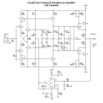
Whoooaa! What a monster!
May i suggest something more simple and functional...
It has very high psrr, thd = 0.0002% (20khz,1v,1k) practically independent of source impedance, low dc-offset, simple, output impedance near zero.
It might need refinement in detail.
May i suggest something more simple and functional...
It has very high psrr, thd = 0.0002% (20khz,1v,1k) practically independent of source impedance, low dc-offset, simple, output impedance near zero.
It might need refinement in detail.
Attachments
Michael,
Your feedback JFET buffer is a clever design! 😎
When extremly controlled DC-offset is not a big issue, I suppose it would work well with selected and thermally coupled BF245C's, BF861C's or similar and then being a low cost design as well.
- Klaus
Your feedback JFET buffer is a clever design! 😎
When extremly controlled DC-offset is not a big issue, I suppose it would work well with selected and thermally coupled BF245C's, BF861C's or similar and then being a low cost design as well.
- Klaus
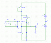
It's not really a feedback design. It's a constant voltage, constant current design, sadly not mine. The principle is from steven.
The idea is, a device having no voltage/current fluctuations does not distort by principle.
Mike
The idea is, a device having no voltage/current fluctuations does not distort by principle.
Mike
As usual, it's a matter of viewpoint wether we call it feedback or not 😉
Actually I made my way through the circuit regarding the PNP as the error amplifier which tries to establish a constant Vds accross the FET by controlling the NPN current sink. This controlled current sink also gives the low Zout of 0.1R, rising from ~20kHz with a 6dB/oct slope to ~10R at 10Mhz, as per sim (also getting your ballpark THD numbers). All this confirmes the feedback view, giving the gain values of a single simple common emitter stage. It is not direct signal feedback, of course, rather it is somewhat indirect via the constant Vds and constant Id.
Do you have a reference/link to the circuit (I don't know which Steven is meant)?
- Klaus
Mike,
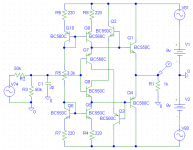
Circuit 1 might not be up to driving low z headphones but circuit 2 gets my vote but I would attach the collectors of Q7 nd Q8 to the rails.
Jam
Circuit 1 might not be up to driving low z headphones but circuit 2 gets my vote but I would attach the collectors of Q7 nd Q8 to the rails.
Jam
MikeB said:
May i suggest something more simple and functional...
It has very high psrr,
thd = 0.0002% (20khz,1v,1k)
practically independent of source impedance,
low dc-offset, simple,
output impedance near zero.
It might need refinement in detail.
Thanks for post that one, symasym-Mike 😎MikeB said:It's not really a feedback design.
It's a constant voltage, constant current design, sadly not mine.
The principle is from steven.
The idea is, a device having no voltage/current fluctuations does not distort by principle.
Mike
It is a remarkable circuit. I am going to say however invented it is a MASTER.
-----------------
I started out using 2SK170BL, at ~10 mA CCS. And for a 1 kohm load.
After some tweaking I ran THD, FFT and AC-Analys.
Boy what performance!
Compared to other circuits I have simulated.
-----------------
Then I switched to 2SK170GR model. 4.8 mA constant current.
As can be seen in my attached circuit.
I chose 2SA970 (high gain) for NPN and BCP56-16 for NPN.
BCP56-16 is a modern SOT223 (max 1.5W), basically with same characteristics as BC639-16.
The ouput level is considerable in my simulation:
Load is 5kOhm.
14.14 Vpeak (out of 20 max supply)
2.83 mA peak output current, almost 60% of 4.8 mA
I have used 22pF at input, to roll off -3dB at:
~ 2.2 MHz
( For practical use, if not having super PCB board layout,
I would recommend to change C2 to 100pF,
which would give a rolloff at ~ 480 KHz )
FFT shows nice spectrum, at the above OUTPUT:
2nd: -101 dB
3rd: -116 dB
4th: -136 dB
5th: -142 dB
..and the rest is below -150 dB
This circuit shows one unusual thing:
It puts out a tiny bit HIGHER Voltage, than the input

This is why I have added a small ( 75 Ohm ) resistor,
to drop to same output level.
As mentioned, it has a very good PSRR.
This is typical for circuits that uses CCS, constant current sources in vital parts of the amplifier.
There is for example a high correlation between
The Price and The PSRR ratio in good audio OP-Amps.
Study datasheets and you see this is a fact.
Regards
lineup
Attachments

Seconded! My hat's off to the designer.lineup said:Thanks for post that one, symasym-Mike 😎
It is a remarkable circuit. I am going to say however invented it is a MASTER.
This slight increase comes from the sligthly lower current in the bottom FET. I've fiddled with the circuit a bit, added a emitter follower in front of the PNP which allows more current (=more bandwidth) in the "error amp", plus it unloads this fluctuating current from the top FET ---> even better perfomance.... this circuit really seems to have some potential. Another neat feature is that it works down to I/O-voltages close to the neg. supply.This circuit shows one unusual thing:
It puts out a tiny bit HIGHER Voltage, than the input
This is why I have added a small ( 75 Ohm ) resistor,
to drop to same output level.
- Klaus
I might be wrong, but it seems the relation between the BJT and the FET is positive feedback instead of negative feedback.

MikeB said:Or, may i introduce "Cadibu"?
Similar performance, but less good dc-offset... But, cheaper.
Mike
MikeB, I'm interested in this Diamond Buffer Output Stage. What is the use of Q2 and Q3? And since the input is BJT, would not the high input bias cause some instability issues when used with a high resistance pot?
Surprise
TzeYang,
I am plesantly surprised to see a Penangnite visiting this forum. I am an ex-Penangnite, but still a Malaysian.
cheers.
TzeYang,
I am plesantly surprised to see a Penangnite visiting this forum. I am an ex-Penangnite, but still a Malaysian.
cheers.
jam said:Mike,
Circuit 1 might not be up to driving low z headphones but circuit 2 gets my vote but I would attach the collectors of Q7 nd Q8 to the rails.
Jam
q2/3 between the collectors of q7/8 and the rails are the difference to a normal diamondbuffer and are floating cascodes. These heavily improve performance of the buffer.
Steven is a member of this forum.
Mike
Hi, MikeB,
I saw some make diamond buffer by attaching collector of Q8 to emitor of Q1 (C-Q7 to E-Q4), instead to rails. What properties are improved this way?
I saw some make diamond buffer by attaching collector of Q8 to emitor of Q1 (C-Q7 to E-Q4), instead to rails. What properties are improved this way?
Mike! So can you expain more details about the difference?😎q2/3 between the collectors of q7/8 and the rails are the difference to a normal diamondbuffer and are floating cascodes. These heavily improve performance of the buffer.
Thanks!
- Status
- Not open for further replies.
- Home
- Amplifiers
- Solid State
- best voltage follower, discrete opamp and whatnot