Hi jcx.
An apology is due.
I did not think it could be the op-amp so I eventually found I had 1uF on the output stage instead of 1nF.
It does not oscillate then, but it is right on the edge of stability; as shown by the oscillation with 1uF.
I do not have the same Mosfets as you but the amplifier is like an inductor from 100Hz up, which is a much lower frequency than with other Mosfet designs.
Look at the 1A 5kHz output impedance test you mentioned.
As I suggested there is a spike before 250nS, and the output terminal potential is in quadrature with the drive current. I got 350 microhms. Then when I turned up the iteration resolution, once again there was oscillation.
You need to be careful with this one.
Cheers ........ Graham
jcx said:anyone spending >10% of their engineering effort on simulation are probably wasting that time
it depends. I know of production cpus that were engineered from beginning to end on simulators.
so it can be done (easier in the digital world than in the analog world) but it doesn't need to be the only way.
Hi Millwood,
Yes, but an inductive characteristic is more due to topology than the devices within it, or its simulation.
Cheers ........... graham.
Yes, but an inductive characteristic is more due to topology than the devices within it, or its simulation.
Cheers ........... graham.
Hi jcx,
maybe whether doing most design on spice pays off depends on how much prior physical work experience one has. I have already spent thousands of hours working with physical circuits, yet, personally I know that simulators, (mcdemo deserves most credit) have saved me much more time than I would have otherwise spent. I think the ratio is at least completely flipped for me and maybe even multiplied by additional 2 or 3. So, the designs I have, without simulators would probably have taken a few tens of thousands of hours to devise, yet with them have taken only a few hundred. Much of it is that I can relax not having to concentrate working with physical parts, and that allows my creativity to flow. Also, I do not have to become mentally fatigued simulating circuit operation in my head from scratch, but can follow the process of the simulator. Therefore, I have much more power to create.
maybe whether doing most design on spice pays off depends on how much prior physical work experience one has. I have already spent thousands of hours working with physical circuits, yet, personally I know that simulators, (mcdemo deserves most credit) have saved me much more time than I would have otherwise spent. I think the ratio is at least completely flipped for me and maybe even multiplied by additional 2 or 3. So, the designs I have, without simulators would probably have taken a few tens of thousands of hours to devise, yet with them have taken only a few hundred. Much of it is that I can relax not having to concentrate working with physical parts, and that allows my creativity to flow. Also, I do not have to become mentally fatigued simulating circuit operation in my head from scratch, but can follow the process of the simulator. Therefore, I have much more power to create.
PS: Though I still prefer tinkering with microcap for circuits with less than 50 parts, I have found LTspice to be great for large circuits.
JFET INPUT FIRST EFFORT
Graham,
I duplicated you Spice simulation results to have a reference design that I could breadboard. Thanks again for your hard work. I'll remember your emphasis on hf second cycles where base junction carrier retention can prematurely cause slew rate limiting unless the charges are pulled out by a powerful driver stage.
I would also like to develop a complementary differential design using JFETs at the input and perhaps the VAS for comparison. JFETs have the mystique of low noise and fine detail. The attached schematic is two nights work of downloading LTspice, models, and a first topology. Better ideas are appreciated.
WHAT ARE THE BEST LOW NOISE SINGLE PACKAGE MATCHED BIPOLAR PAIRS FOR:
(1) NPN front-end current sources; 4-10 ma
(2) PNP front-end current sources; 4-10 ma
(3) NPN front-end input differential;
(4) NPN 2nd stage current source of 200ma - 400ma;
(5) PNP for front-end differential pairs;
ARE THERE ANY HIGH CURRENT P-JFETS AND N-JFETS THAT CAN BE USED FOR A SECOND STAGE VAS?
Attachments

"Fred,
You seem to be the one the major issue with the sim #, why don't you measure one of these devices for us?"
Maybe because I am not the one claiming parameters that are not shown on the data sheet. I have looked at these type trends for devices that I use like the IRF 150 and a few of the IXYS mosfets. I can't understand why you would not have ordered some to measure yourself if you are convinced the device has that good a transconductance at 2 or 3 amps. Afraid of what you might find? I am sure someone will get around to it. Maybe Mr. Pass or Mr. Hanson has some experience with similar mosfets.
"it depends. I know of production cpus that were engineered from beginning to end on simulators."
With millions of transistors I don't think you are going to find many that aren't. Having a good friend in the telecom industry who has been an IC designer long enough (over 25 years) to have done both, I can tell you that designs done with only simulators by guys with no experience in physical breadboarding scare him. His experience with the finding the gotya's of actual design prototypes by designers, who grew up on simulation tools, keeps him pretty busy helping to fix these "simulated" designs.
I like Spice for playing with 'what if' type changes and things like filter design. It is a time saver and let's me spend the time on the bench measuring something that is pretty well in the neighborhood of what I want for a circuit. Using it to predict distortion or troubleshoot a problem seen on the bench is generally a lost cause. If people will actually build what they simulate and compare the results they will be surprised. I have seen all kinds of line level preamp circuits being modeled without a capacitive load in the model to simulate the cable capacitance the circuit is driving. Seen many models with power supply and ground impedances included? Parasitic capacitance and inductance? Parasitic inductance and ESR for capacitors in power supply circuits? All off these things are important in how a circuit works. A basic schematic is not a representation of an actual circuit with these parasitics included. There is no substitute for reality in the final analysis. Even if Spice were perfect (and it isn't), without the experience of building circuits you will probably never know enough to make an accurate model of things that make the difference in a good verses bad PCB layout which has a very big effect on what an audio circuit sounds like.
Hi Linesource,
I have a couple of questions about the attached schematic in post #146.
I will focuse on the upper half in my following questions.
What is the idea by cross connecting the cascodes gate to the opposit lower J-FET's Source?
The Miller capacitance seem to me acting in a negative way.
What is the benefit of using doubble curren mirror?
And what is the benefit by connecting Q25 emitter to the input circuit?
There seem to be some 220 mA running through Q11 (15V-0,65Vbe/56 Ohm?), what current are you (as I'm a bit unsure about the circuits function..) suppose to drive through Q25 with emitter connected to the current mirror?
Further on why using R10 with value 20000 Ohm, if the current mirror is programmed to 220 mA, it would equal 4400 Volt over R10 if there is going to be any 220 mA, otherwise I don't understand the use of current mirror Q11 and Q19?
Cheers! 🙂
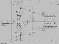
LineSource,
You’ve got a few ok parts and pieces there but they don’t hang together yet – not even in sim ( for posts 146 and 149)
Current mirrors/sources are seldom made with matched monolithic transistors in audio power amps, current/voltage limits of the few types available and substrate parasitic effects make them not worth the bother compared to discretes with a little resistive emitter degeneration – the discretes can be hand matched and/or current balance trimmed with a pot – and that’s even hardly necessary with 6-700 mV across the degeneration R
The 2nd stage/VAS is totally confused, if you mean to use a folded cascode type design you need to remember the dynamic output current is only that of the 1st stage and compare with the worst case driver base current need – and figure out the right bias arrangement too – I think you’re trying for something similar to: http://www.ne.jp/asahi/evo/amp/J200K1529/report.htm (no I can’t read the text but as much as I can “read” the schematics they seem plausible and show quite a few options, fig 13 looks a lot like where I think you’re intending to go)
The driver/output stage needs a bias source – and given the apparent willingness to waste power for high voltage supply overhead with the +/- 15 V output supply there is no reason not to use one that directly senses and regulates the emitter R voltage to control the class A output and bypass thermal coupling/compensation issues altogether
A way to improve dist # is to change the output from the discrete Darlingtons to Sziklai/CFP – they can perform well in Class A outputs (and only class A due to complicated turn on/off behavior that compromises their AB/B usefulness) – potential stability problems may also be reduced by the specifics of your nearly pure resistive load
In other words, your circuit is complex. An accurate sim on
this is vaguely similar to invading Russia in winter.
this is vaguely similar to invading Russia in winter.
Man ....... I though it was just me!
"In other words, your circuit is complex. An accurate sim on this is vaguely similar to invading Russia in winter." -NP
Then, perhaps the it's maiden voyage should be playing a recording of the Shostakovich Symphony No. 7 in C. I had the misfortune to sit through this played by the Dallas Symphony one evening. I will leave to the scholarly to see why chose that one.
'Current mirrors/sources are seldom made with matched monolithic transistors in audio power amps, current/voltage limits of the few types available and substrate parasitic effects make them not worth the bother compared to discretes with a little resistive emitter degeneration" -jcx
What current/voltage limits? He has them on the front end of an amp with 10 or 15 volt rails running at a few milliamps. The Toshiba 2SC3381 and 2SA1349 are 80 volt 200mW parts and are recommended for "current mirror applications of the front end of the first stages of pre, main power amps" according to the Toshiba data sheet........ Emitter degeneration is a good idea and can be used with monolithic pairs as well. If parasitic effects for monolithic transistors are such a concern I don't see how you can get away with the J109s and K389s
For a circuit topology with as intimate coupling as current mirror I really wonder if parasitics are really worth worrying about, or if jcx is just trying to sound scholarly. I believe the substrate to emitter voltages are very small even with some emitter degeneration. I have used thse devices as the diff pair for an ASKA 55 quite successfully. You have many more important things to worry about with the VAS and output stage bias.
I will still say, that building a voltage amplifier is overkill and unnecessary, since the load is a pure resistance. Building a current amplifier is more suited and will not be that complex.
I do not have a readymade "go-for-it" finished plan, but I am thinking in the lines of this:
http://www.diyaudio.com/forums/showthread.php?postid=371967#post371967
Or the 8Watt amplifier from Hiraga. BUT with a twist, since it does put out voltage. The global feedback have to go, and other local feedback "procedures" must be implemented.
Hi LineSource,
I find it difficult to understand why you would wish to attempt such a complicated circuit.
You will need approx 100 ohms between the BD139 and BD140 emitters, for otherwise the output devices will not turn off quickly enough.
Why do you have cascoded mirrors; see note I have attached. Note that you would have to turn my 'A' around to use it in your circuit.
Have you got it running on a simulator yet ?
Cheers ............. Graham.
Attachments
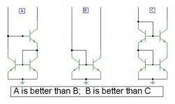
Graham,
A is a Wilson current mirror, B is standard current mirror, and C is a cascoded current mirror.
The Wilson current mirror has better DC accuracy than does a standard current mirror, so in that sense is better. However, it relies upon a short feedback loop for its improved accuracy and may not sound better for audio.
But why do you say that a standard current mirror is "better" than a cascoded current mirror? The standard mirror is simpler, but suffers much more from the Early effect than a cascoded mirror.
Thanks,
Charles Hansen
You folks have the 'current mirror' concept right, BUT they can be a problem by amplifying their own noise. Degeneration resistors in the devices closest to the supply would help keep the potential noise contribution lower.
Jfet Cascode + Cascode Current Source
Graham, Charles Thanks for staying with my 25W 1 ohm thread.
There is a mystique about complementary JFET front-ends and separate current sources for each driver stage as perhaps the best topology for low noise and high detail at low power levels that I want to test for myself. Since I've only had a couple hours to download LTspice and search for transistor models, discussing ideas for each stage seems like the best path.
Input stage: JFET cascodes should reduce the input capacitance below 50pF and also reduce distortion by 2x-3x at low outputs. Using a balanced input should reduce distortion by another 2-3x.
I want to find out if I can hear the difference between a high impedance current source and resistors. A current mirror has Rout ~ ro, both the Wilson and cascode have Rout ~ hfe/2 * ro, and the cascode has balanced voltage drops.
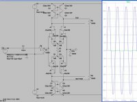
Attached a complementary JFET cascode input stage with complementary cascode current mirrors. 0.1V input, 11V output.
Graham, Charles Thanks for staying with my 25W 1 ohm thread.
There is a mystique about complementary JFET front-ends and separate current sources for each driver stage as perhaps the best topology for low noise and high detail at low power levels that I want to test for myself. Since I've only had a couple hours to download LTspice and search for transistor models, discussing ideas for each stage seems like the best path.
Input stage: JFET cascodes should reduce the input capacitance below 50pF and also reduce distortion by 2x-3x at low outputs. Using a balanced input should reduce distortion by another 2-3x.
I want to find out if I can hear the difference between a high impedance current source and resistors. A current mirror has Rout ~ ro, both the Wilson and cascode have Rout ~ hfe/2 * ro, and the cascode has balanced voltage drops.
Attached a complementary JFET cascode input stage with complementary cascode current mirrors. 0.1V input, 11V output.
Attachments
- Status
- Not open for further replies.
- Home
- Amplifiers
- Solid State
- best topo for 25W class A into 1 ohm resistive load?